
Datasheet
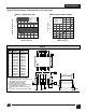


TNY253/254/255
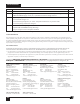
11
D
4/03
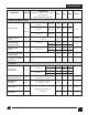
Conditions
Parameter Symbol
SOURCE = 0 V; T
J
= -40 to 125 °C
See Figure 14
(Unless Otherwise Specified)
di/dt = 12.5 mA/µs
T
J
= 25 °C
di/dt = 25 mA/µs
T
J
= 25 °C
di/dt = 80 mA/µs
T
J
= 25 °C
135 150 165
230 255 280
255 280 310
170 240
170 215
200 250
100 150
125 135 145
70
31 36
50 60
23 27
37 45
50
700
50
50
I
LIMIT
Note F
I
INIT
t
LEB
t
ILD
R
DS(ON)
I
DSS
BV
DSS
t
R
t
F
mA
mA
ns
ns
°C
°C
Ω
µA
V
ns
ns
Current Limit
Initial Current
Limit
Leading Edge
Blanking Time
Current Limit
Delay
Thermal Shutdown
Temperature
Thermal Shutdown
Hysteresis
ON-State
Resistance
OFF-State Drain
Leakage Current
Breakdown
Voltage
Rise Time
Fall Time
Min
Typ
Max
Units
CIRCUIT PROTECTION
OUTPUT
V
BP
= 6.2 V, V
EN
= 0 V,
V
DS
= 560 V, T
J
= 125 °C
T
J
= 25 °C
T
J
= 100 °C
T
J
= 25 °C
T
J
= 100 °C
TNY253/TNY254
I
D
= 25 mA
Measured with Figure 10
Schematic.
TNY253
TNY254
TNY255
V
BP
= 6.2 V, V
EN
= 0 V,
I
DS
= 100 µA, T
J
= 25 °C
TNY253
TNY254
TNY255
TNY253
TNY254
TNY255
T
J
= 25 °C
See Note G
TNY255
I
D
= 33 mA
See Figure 17
T
J
= 25 °C
T
J
= 25 °C
0.65 x
I
LIMIT(MIN)