
Data Sheet


Control interface VL53L1X
20/35 DocID031281 Rev 2
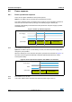
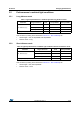
Figure 13. VL53L1X data format (write)
As data are received by the slave, they are written bit-by-bit to a serial/parallel register. After
each data byte has been received by the slave, an acknowledge is generated, the data are
then stored in the internal register addressed by the current index.
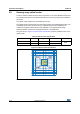
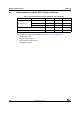
During a read message, the contents of the register addressed by the current index is read
out in the byte following the device address byte. The contents of this register are parallel
loaded into the serial/parallel register and clocked out of the device by the falling edge of
SCL.
Figure 14. VL53L1X data format (read)
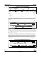
At the end of each byte, in both read and write message sequences, an acknowledge is
issued by the receiving device (that is, the VL53L1X for a write and the host for a read).
A message can only be terminated by the bus master, either by issuing a stop condition or
by a negative acknowledge (that is, not pulling the SDA line low) after reading a complete
byte during a read operation.
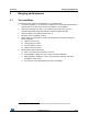
The interface also supports auto-increment indexing. After the first data byte has been
transferred, the index is automatically incremented by 1. The master can therefore send
data bytes continuously to the slave until the slave fails to provide an acknowledge or the
master terminates the write communication with a stop condition. If the auto-increment
feature is used the master does not have to send address indexes to accompany the data
bytes.
Figure 15. VL53L1X data format (sequential write)
VL53L1X acknowledges
Acknowledge from VL53L1X
S AsADDRESS[7:0]
INDEX[15:8]
As DATA[7:0] As
P
0x52 (write)
Start
Stop
valid address
As
INDEX[7:0]
S As
ADDRESS[7:0]
INDEX[7:0]
As P
0x52 (write)
S As
ADDRESS[7:0]
Am
DATA[7:0]
P
0x53 (read)
INDEX[15:8]
As
PAs
DATA[7:0]
As
DATA[7:0]
As
DATA[7:0]
S As
ADDRESS[7:0]
INDEX[7:0]
As P
0x52 (write)
INDEX[15:8]
As