
Data Sheet


UM10204 All information provided in this document is subject to legal disclaimers. © NXP Semiconductors N.V. 2014. All rights reserved.
User manual Rev. 6 — 4 April 2014 60 of 64
NXP Semiconductors
UM10204
I
2
C-bus specification and user manual
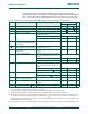
7.5 Wiring pattern of the bus lines
In general, the wiring must be chosen so that crosstalk and interference to/from the bus
lines is minimized. The bus lines are most susceptible to crosstalk and interference at the
HIGH level because of the relatively high impedance of the pull-up devices.
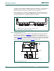
If the length of the bus lines on a PCB or ribbon cable exceeds 10 cm and includes the
V
DD
and V
SS
lines, the wiring pattern should be:
SDA _______________________
V
DD
________________________
V
SS
________________________
SCL _______________________
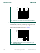
If only the V
SS
line is included, the wiring pattern should be:
SDA _______________________
V
SS
________________________
SCL _______________________
These wiring patterns also result in identical capacitive loads for the SDA and SCL lines.
If a PCB with a V
SS
and/or V
DD
layer is used, the V
SS
and V
DD
lines can be omitted.
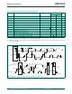
If the bus lines are twisted-pairs, each bus line must be twisted with a V
SS
return.
Alternatively, the SCL line can be twisted with a V
SS
return, and the SDA line twisted with
a V
DD
return. In the latter case, capacitors must be used to decouple the V
DD
line to the
V
SS
line at both ends of the twisted pairs.
If the bus lines are shielded (shield connected to V
SS
), interference is minimized.
However, the shielded cable must have low capacitive coupling between the SDA and
SCL lines to minimize crosstalk.