
Data Sheet


UM10204 All information provided in this document is subject to legal disclaimers. © NXP Semiconductors N.V. 2014. All rights reserved.
User manual Rev. 6 — 4 April 2014 58 of 64
NXP Semiconductors
UM10204
I
2
C-bus specification and user manual
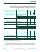
The switched pull-up circuit in Figure 44 is for a supply voltage of V
DD
=5V± 10 % and a
maximum capacitive load of 400 pF. Since it is controlled by the bus levels, it needs no
additional switching control signals. During the rising/falling edges, the bilateral switch in
the HCT4066 switches pull-up resistor R
p2
on/off at bus levels between 0.8 V and 2.0 V.
Combined resistors R
p1
and R
p2
can pull up the bus line within the maximum specified
rise time (t
r
) of 300 ns.
Series resistors R
s
are optional. They protect the I/O stages of the I
2
C-bus devices from
high-voltage spikes on the bus lines, and minimize crosstalk and undershoot of the bus
line signals. The maximum value of R
s
is determined by the maximum permitted voltage
drop across this resistor when the bus line is switched to the LOW level in order to switch
off R
p2
.
Additionally, some bus buffers contain integral rise time accelerators. Stand-alone rise
time accelerators are also available.
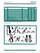
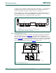
7.3 Series protection resistors
As shown in Figure 45, series resistors (R
s
) of, for example, 300 Ω can be used for
protection against high-voltage spikes on the SDA and SCL lines (resulting from the
flash-over of a TV picture tube, for example). If series resistors are used, designers must
add the additional resistance into their calculations for R
p
and allowable bus capacitance.
The required noise margin of 0.1V
DD
for the LOW level, limits the maximum value of R
s
.
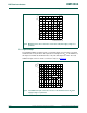
R
s(max)
as a function of R
p
is shown in Figure 46. Note that series resistors affect the
output fall time.
Fig 45. Series resistors (R
s
) for protection against high-voltage spikes
mbc627
SDA
SCL
DEVICE
V
DD
V
DD
I
2
C
R
s
R
s
R
s
R
s
R
p
R
p
DEVICE
I
2
C