
Data Sheet


UM10204 All information provided in this document is subject to legal disclaimers. © NXP Semiconductors N.V. 2014. All rights reserved.
User manual Rev. 6 — 4 April 2014 56 of 64
NXP Semiconductors
UM10204
I
2
C-bus specification and user manual
The designer now has the minimum and maximum value of R
p
that is required to meet the
timing specification. Portable designs with sensitivity to supply current consumption can
use a value toward the higher end of the range in order to limit I
DD
.
7.2 Operating above the maximum allowable bus capacitance
Bus capacitance limit is specified to limit rise time reductions and allow operating at the
rated frequency. While most designs can easily stay within this limit, some applications
may exceed it. There are several strategies available to system designers to cope with
excess bus capacitance.
• Reduced f
SCL
(Section 7.2.1): The bus may be operated at a lower speed (lower f
SCL
).
• Higher drive outputs (Section 7.2.2): Devices with higher drive current such as those
rated for Fast-mode Plus can be used (PCA96xx).
• Bus buffers (Section 7.2.3): There are a number of bus buffer devices available that
can divide the bus into segments so that each segment has a capacitance below the
allowable limit, such as the PCA9517 bus buffer or the PCA9546A switch.
• Switched pull-up circuit (Section 7.2.4): A switched pull-up circuit can be used to
accelerate rising edges by switching a low value pull-up alternately in and out when
needed.
7.2.1 Reduced f
SCL
To determine a lower allowable bus operating frequency, begin by finding the t
LOW
and
t
HIGH
of the most limiting device on the bus. Refer to individual component data sheets for
these values. Actual rise time (t
r
) depends on the RC time constant. The most limiting fall
time (t
f
) depends on the lowest output drive on the bus. Be sure to allow for any devices
that have a minimum t
r
or t
f
. Refer to Equation 3 for the resulting f
max
.
(3)
Remark: Very long buses must also account for time of flight of signals.
Actual results are slower, as real parts do not tend to control t
LOW
and t
HIGH
to the
minimum from 30 % to 70 %, or 70 % to 30 %, respectively.
7.2.2 Higher drive outputs
If higher drive devices like the PCA96xx Fast-mode Plus or the P82B bus buffers are
used, the higher strength output drivers sink more current which results in considerably
faster edge rates, or, looked at another way, allows a higher bus capacitance. Refer to
individual component data sheets for actual output drive capability. Repeat the calculation
above using the new values of C
b
, R
p
, t
r
and t
f
to determine maximum frequency. Bear in
mind that the maximum rating for f
SCL
as specified in Table 10 (100 kHz, 400 kHz and
1000 kHz) may become limiting.
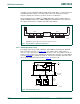
7.2.3 Bus buffers, multiplexers and switches
Another approach to coping with excess bus capacitance is to divide the bus into smaller
segments using bus buffers, multiplexers or switches. Figure 43
shows an example of a
bus that uses a PCA9515 buffer to deal with high bus capacitance. Each segment is then
allowed to have the maximum capacitance so the total bus can have twice the maximum
f
max
1
t
LOW min()
t
HIGH mi n()
t
r actual()
t
f actual()
+++
-------------------------------------------------------------------------------------------------------------
=