
Data Sheet


UM10204 All information provided in this document is subject to legal disclaimers. © NXP Semiconductors N.V. 2014. All rights reserved.
User manual Rev. 6 — 4 April 2014 55 of 64
NXP Semiconductors
UM10204
I
2
C-bus specification and user manual
7. Electrical connections of I
2
C-bus devices to the bus lines
7.1 Pull-up resistor sizing
The bus capacitance is the total capacitance of wire, connections and pins. This
capacitance limits the maximum value of R
p
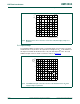
due to the specified rise time. Figure 41
shows R
p(max)
as a function of bus capacitance.
Consider the V
DD
related input threshold of V
IH
=0.7V
DD
and V
IL
=0.3V
DD
for the
purposes of RC time constant calculation. Then V(t) = V
DD
(1 − e
−t/RC
), where t is the
time since the charging started and RC is the time constant.
V(t1) = 0.3 × V
DD
=V
DD
(1 − e
−t1 / RC
); then t1 = 0.3566749 × RC
V(t2) = 0.7 × V
DD
=V
DD
(1 − e
−t2 / RC
); then t2 = 1.2039729 × RC
T=t2− t1 = 0.8473 × RC
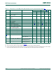
Figure 41
and Equation 1 shows maximum R
p
as a function of bus capacitance for
Standard-, Fast- and Fast-mode Plus. For each mode, the R
p(max)
is a function of the
rise time maximum (t
r
) from Table 10 and the estimated bus capacitance (C
b
):
(1)
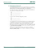
The supply voltage limits the minimum value of resistor R
p
due to the specified minimum
sink current of 3 mA for Standard-mode and Fast-mode, or 20 mA for Fast-mode Plus.
R
p(min)
as a function of V
DD
is shown in Figure 42. The traces are calculated using
Equation 2
:
(2)
R
pmax()
t
r
0.8473 C
b
×
-----------------------------
=
(1) Standard-mode
(2) Fast-mode
(3) Fast-mode Plus
(1) Fast-mode and Standard-mode
(2) Fast-mode Plus
Fig 41. R
p(max)
as a function of bus capacitance Fig 42. R
p(min)
as a function of V
DD
40
80
120
R
p(max)
(kΩ)
0
aaa-012677
C
b
(pF)
0 600400200
(1)
(2)
(3)
2
3
1
4
5
R
p(min)
(kΩ)
0
V
DD
(V)
020168124
aaa-012678
3 mA
20 mA
(1)
(2)
R
pmin()
V
DD
V
OL max()
–
I
OL
--------------------------------------
=