
Data Sheet


UM10204 All information provided in this document is subject to legal disclaimers. © NXP Semiconductors N.V. 2014. All rights reserved.
User manual Rev. 6 — 4 April 2014 52 of 64
NXP Semiconductors
UM10204
I
2
C-bus specification and user manual
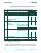
[1] All values referred to V
IH(min)
and V
IL(max)
levels (see Table 11).
[2] For bus line loads C
b
between 100 pF and 400 pF the timing parameters must be linearly interpolated.
[3] A device must internally provide a data hold time to bridge the undefined part between V
IH
and V
IL
of the falling edge of the SCLH signal.
An input circuit with a threshold as low as possible for the falling edge of the SCLH signal minimizes this hold time.
Table 12. Characteristics of the SDAH, SCLH, SDA and SCL bus lines for Hs-mode I
2
C-bus devices
[1]
Symbol Parameter Conditions C
b
= 100 pF (max) C
b
= 400 pF
[2]
Unit
Min Max Min Max
f
SCLH
SCLH clock frequency 0 3.4 0 1.7 MHz
t
SU;STA
set-up time for a repeated
START condition
160 - 160 - ns
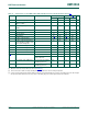
t
HD;STA
hold time (repeated) START
condition
160 - 160 - ns
t
LOW
LOW period of the SCL clock 160 - 320 - ns
t
HIGH
HIGH period of the SCL clock 60 - 120 - ns
t
SU;DAT
data set-up time 10 - 10 - ns
t
HD;DAT
data hold time 0
[3]
70 0
[3]
150 ns
t
rCL
rise time of SCLH signal 10 40 20 80 ns
t
rCL1
rise time of SCLH signal after a
repeated START condition and
after an acknowledge bit
10 80 20 160 ns
t
fCL
fall time of SCLH signal 10 40 20 80 ns
t
rDA
rise time of SDAH signal 10 80 20 160 ns
t
fDA
fall time of SDAH signal 10 80 20 160 ns
t
SU;STO
set-up time for STOP condition 160 - 160 - ns
C
b
[2]
capacitive load for each bus line SDAH and SCLH lines - 100 - 400 pF
SDAH + SDA line and
SCLH + SCL line
- 400 - 400 pF
V
nL
noise margin at the LOW level for each connected device
(including hysteresis)
0.1V
DD
-0.1V
DD
-V
V
nH
noise margin at the HIGH level for each connected device
(including hysteresis)
0.2V
DD
-0.2V
DD
-V