
Data Sheet


UM10204 All information provided in this document is subject to legal disclaimers. © NXP Semiconductors N.V. 2014. All rights reserved.
User manual Rev. 6 — 4 April 2014 51 of 64
NXP Semiconductors
UM10204
I
2
C-bus specification and user manual
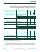
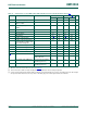
capacitive bus loads between 100 pF and 400 pF, the timing parameters must be
interpolated linearly. Rise and fall times are in accordance with the maximum propagation
time of the transmission lines SDAH and SCLH to prevent reflections of the open ends.
[1] Devices that use non-standard supply voltages which do not conform to the intended I
2
C-bus system levels must relate their input levels
to the V
DD
voltage to which the pull-up resistors R
p
are connected.
[2] Devices that offer the level shift function must tolerate a maximum input voltage of 5.5 V at SDA and SCL.
[3] For capacitive bus loads between 100 pF and 400 pF, the rise and fall time values must be linearly interpolated.
[4] If their supply voltage has been switched off, SDAH and SCLH I/O stages of Hs-mode slave devices must have floating outputs. Due to
the current-source output circuit, which normally has a clipping diode to V
DD
, this requirement is not mandatory for the SCLH or the
SDAH I/O stage of Hs-mode master devices. This means that the supply voltage of Hs-mode master devices cannot be switched off
without affecting the SDAH and SCLH lines.
[5] Special purpose devices such as multiplexers and switches may exceed this capacitance because they connect multiple paths together.
Table 11. Characteristics of the SDAH, SCLH, SDA and SCL I/O stages for Hs-mode I
2
C-bus devices
Symbol Parameter Conditions Hs-mode Unit
Min Max
V
IL
LOW-level input voltage −0.5 0.3V
DD
[1]
V
V
IH
HIGH-level input voltage 0.7V
DD
[1]
V
DD
+0.5
[2]
V
V
hys
hysteresis of Schmitt trigger inputs 0.1V
DD
[1]
-V
V
OL
LOW-level output voltage (open-drain) at 3 mA sink current at
SDAH, SDA and SCLH
V
DD
>2V 0 0.4 V
V
DD
≤ 2V 0 0.2V
DD
V
R
onL
transfer gate on resistance for
currents between SDA and SDAH or
SCL and SCLH
V
OL
level; I
OL
=3mA - 50 Ω
R
onH
[2]
transfer gate on resistance between
SDA and SDAH or SCL and SCLH
both signals (SDA and SDAH, or SCL
and SCLH) at V
DD
level
50 - kΩ
I
CS
pull-up current of the SCLH
current-source
SCLH output levels between 0.3V
DD
and
0.7V
DD
312mA
t
rCL
rise time of SCLH signal output rise time (current-source enabled)
with an external pull-up current source of
3mA
capacitive load from 10 pF to 100 pF 10 40 ns
capacitive load of 400 pF
[3]
20 80 ns
t
fCL
fall time of SCLH signal output fall time (current-source enabled)
with an external pull-up current source of
3mA
capacitive load from 10 pF to 100 pF 10 40 ns
capacitive load of 400 pF
[3]
20 80 ns
t
fDA
fall time of SDAH signal capacitive load from 10 pF to 100 pF 10 80 ns
capacitive load of 400 pF
[3]
20 160 ns
t
SP
pulse width of spikes that must be
suppressed by the input filter
SDAH and SCLH 0 10 ns
I
i
[4]
input current each I/O pin input voltage between 0.1V
DD
and
0.9V
DD
-10μA
C
i
capacitance for each I/O pin
[5]
-10pF