
Data Sheet

UM10204 All information provided in this document is subject to legal disclaimers. © NXP Semiconductors N.V. 2014. All rights reserved.
User manual Rev. 6 — 4 April 2014 50 of 64
NXP Semiconductors
UM10204
I
2
C-bus specification and user manual
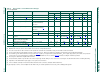
6.2 Hs-mode devices
The I/O levels, I/O current, spike suppression, output slope control and pin capacitance for
I
2
C-bus Hs-mode devices are given in Table 11 . The noise margin for HIGH and LOW
levels on the bus lines are the same as specified for F/S-mode I
2
C-bus devices.
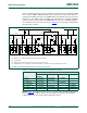
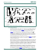
Figure 39
shows all timing parameters for the Hs-mode timing. The ‘normal’ START
condition S does not exist in Hs-mode. Timing parameters for Address bits, R/W
bit,
Acknowledge bit and DATA bits are all the same. Only the rising edge of the first SCLH
clock signal after an acknowledge bit has a larger value because the external R
p
has to
pull up SCLH without the help of the internal current-source.
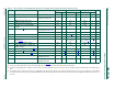
The Hs-mode timing parameters for the bus lines are specified in Table 12
. The minimum
HIGH and LOW periods and the maximum rise and fall times of the SCLH clock signal
determine the highest bit rate.
With an internally generated SCLH signal with LOW and HIGH level periods of 200 ns and
100 ns respectively, an Hs-mode master fulfills the timing requirements for the external
SCLH clock pulses (taking the rise and fall times into account) for the maximum bit rate of
3.4 Mbit/s. So a basic frequency of 10 MHz, or a multiple of 10 MHz, can be used by an
Hs-mode master to generate the SCLH signal. There are no limits for maximum HIGH and
LOW periods of the SCLH clock, and there is no limit for a lowest bit rate.
Timing parameters are independent for capacitive load up to 100 pF for each bus line
allowing the maximum possible bit rate of 3.4 Mbit/s. At a higher capacitive load on the
bus lines, the bit rate decreases gradually. The timing parameters for a capacitive bus
load of 400 pF are specified in Table 12
, allowing a maximum bit rate of 1.7 Mbit/s. For
V
IL
=0.3V
DD
V
IH
=0.7V
DD
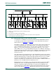
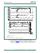
Fig 38. Definition of timing for F/S-mode devices on the I
2
C-bus
002aac938
t
f
70 %
30 %
SDA
t
f
70 %
30 %
S
t
r
70 %
30 %
70 %
30 %
t
HD;DAT
SCL
1 / f
SCL
1
st
clock cycle
70 %
30 %
70 %
30 %
t
r
t
VD;DAT
cont.
cont.
SDA
SCL
t
SU;STA
t
HD;STA
Sr
t
SP
t
SU;STO
t
BUF
P S
t
HIGH
9
th
clock
t
HD;STA
t
LOW
70 %
30 %
t
VD;ACK
9
th
clock
t
SU;DAT