
Data Sheet

xxxxxxxxxxxxxxxxxxxxx xxxxxxxxxxxxxxxxxxxxxxxxxx xxxxxxx x x x xxxxxxxxxxxxxxxxxxxxxxxxxxxxxx xxxxxxxxxxxxxxxxxxx xx xx xxxxx
xxxxxxxxxxxxxxxxxxxxxxxxxxx xxxxxxxxxxxxxxxxxxx xxxxxx xxxxxxxxxxxxxxxxxxxxxxxxxxxxxxxxxxx xxxxxxxxxxxx x x
xxxxxxxxxxxxxxxxxxxxx xxxxxxxxxxxxxxxxxxxxxxxxxxxxxx xxxxx xxxxxxxxxxxxxxxxxxxxxxxxxxxxxxxxxxxxxxxxxxxxxxxxxx xxxxxxxx
xxxxxxxxxxxxxxxxxxxxxxxxx xxxxxxxxxxxxxxxxxxxx xxx
UM10204 All information provided in this document is subject to legal disclaimers. © NXP Semiconductors N.V. 2014. All rights reserved.
User manual Rev. 6 — 4 April 2014 49 of 64
NXP Semiconductors
UM10204
I
2
C-bus specification and user manual
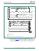
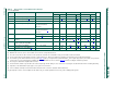
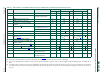
[5] A Fast-mode I
2
C-bus device can be used in a Standard-mode I
2
C-bus system, but the requirement t
SU;DAT
250 ns must then be met. This will automatically be the case if the
device does not stretch the LOW period of the SCL signal. If such a device does stretch the LOW period of the SCL signal, it must output the next data bit to the SDA line
t
r(max)
+t
SU;DAT
= 1000 + 250 = 1250 ns (according to the Standard-mode I
2
C-bus specification) before the SCL line is released. Also the acknowledge timing must meet this
set-up time.
[6] If mixed with Hs-mode devices, faster fall times according to Table 10
are allowed.
[7] The maximum t
f
for the SDA and SCL bus lines is specified at 300 ns. The maximum fall time for the SDA output stage t
f
is specified at 250 ns. This allows series protection
resistors to be connected in between the SDA and the SCL pins and the SDA/SCL bus lines without exceeding the maximum specified t
f
.
[8] In Fast-mode Plus, fall time is specified the same for both output stage and bus timing. If series resistors are used, designers should allow for this when considering bus timing.
[9] Necessary to be backwards compatible to Fast-mode.
[10] The maximum bus capacitance allowable may vary from this value depending on the actual operating voltage and frequency of the application. Section 7.2
discusses techniques
for coping with higher bus capacitances.
[11] t
VD;DAT
= time for data signal from SCL LOW to SDA output (HIGH or LOW, depending on which one is worse).
[12] t
VD;ACK
= time for Acknowledgement signal from SCL LOW to SDA output (HIGH or LOW, depending on which one is worse).