
Data Sheet

xxxxxxxxxxxxxxxxxxxxx xxxxxxxxxxxxxxxxxxxxxxxxxx xxxxxxx x x x xxxxxxxxxxxxxxxxxxxxxxxxxxxxxx xxxxxxxxxxxxxxxxxxx xx xx xxxxx
xxxxxxxxxxxxxxxxxxxxxxxxxxx xxxxxxxxxxxxxxxxxxx xxxxxx xxxxxxxxxxxxxxxxxxxxxxxxxxxxxxxxxxx xxxxxxxxxxxx x x
xxxxxxxxxxxxxxxxxxxxx xxxxxxxxxxxxxxxxxxxxxxxxxxxxxx xxxxx xxxxxxxxxxxxxxxxxxxxxxxxxxxxxxxxxxxxxxxxxxxxxxxxxx xxxxxxxx
xxxxxxxxxxxxxxxxxxxxxxxxx xxxxxxxxxxxxxxxxxxxx xxx
UM10204 All information provided in this document is subject to legal disclaimers. © NXP Semiconductors N.V. 2014. All rights reserved.
User manual Rev. 6 — 4 April 2014 48 of 64
NXP Semiconductors
UM10204
I
2
C-bus specification and user manual
[1] All values referred to V
IH(min)
(0.3V
DD
) and V
IL(max)
(0.7V
DD
) levels (see Table 9).
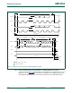
[2] t
HD;DAT
is the data hold time that is measured from the falling edge of SCL, applies to data in transmission and the acknowledge.
[3] A device must internally provide a hold time of at least 300 ns for the SDA signal (with respect to the V
IH(min)
of the SCL signal) to bridge the undefined region of the falling edge of
SCL.
[4] The maximum t
HD;DAT
could be 3.45 μs and 0.9 μs for Standard-mode and Fast-mode, but must be less than the maximum of t
VD;DAT
or t
VD;ACK
by a transition time. This maximum
must only be met if the device does not stretch the LOW period (t
LOW
) of the SCL signal. If the clock stretches the SCL, the data must be valid by the set-up time before it releases
the clock.
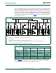
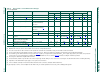
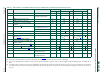
Table 10. Characteristics of the SDA and SCL bus lines for Standard, Fast, and Fast-mode Plus I
2
C-bus devices
[1]
Symbol Parameter Conditions Standard-mode Fast-mode Fast-mode Plus Unit
Min Max Min Max Min Max
f
SCL
SCL clock frequency 0 100 0 400 0 1000 kHz
t
HD;STA
hold time (repeated) START condition After this period, the first
clock pulse is generated.
4.0 - 0.6 - 0.26 - μs
t
LOW
LOW period of the SCL clock 4.7 - 1.3 - 0.5 - μs
t
HIGH
HIGH period of the SCL clock 4.0 - 0.6 - 0.26 - μs
t
SU;STA
set-up time for a repeated START
condition
4.7 - 0.6 - 0.26 - μs
t
HD;DAT
data hold time
[2]
CBUS compatible masters
(see Remark in Section 4.1)
5.0 - - - - - μs
I
2
C-bus devices 0
[3]
-
[4]
0
[3]
-
[4]
0-μs
t
SU;DAT
data set-up time 250 - 100
[5]
-50 -ns
t
r
rise time of both SDA and SCL signals - 1000 20 300 - 120 ns
t
f
fall time of both SDA and SCL
signals
[3][6][7][8]
- 300 20 ×
(V
DD
/5.5V)
300 20 ×
(V
DD
/5.5V)
[9]
120
[8]
ns
t
SU;STO
set-up time for STOP condition 4.0 - 0.6 - 0.26 - μs
t
BUF
bus free time between a STOP and
START condition
4.7 - 1.3 - 0.5 - μs
C
b
capacitive load for each bus line
[10]
- 400 - 400 - 550 pF
t
VD;DAT
data valid time
[11]
-3.45
[4]
-0.9
[4]
-0.45
[4]
μs
t
VD;ACK
data valid acknowledge time
[12]
-3.45
[4]
-0.9
[4]
-0.45
[4]
μs
V
nL
noise margin at the LOW level for each connected device
(including hysteresis)
0.1V
DD
-0.1V
DD
-0.1V
DD
-V
V
nH
noise margin at the HIGH level for each connected device
(including hysteresis)
0.2V
DD
-0.2V
DD
-0.2V
DD
-V