
Data Sheet

xxxxxxxxxxxxxxxxxxxxx xxxxxxxxxxxxxxxxxxxxxxxxxx xxxxxxx x x x xxxxxxxxxxxxxxxxxxxxxxxxxxxxxx xxxxxxxxxxxxxxxxxxx xx xx xxxxx
xxxxxxxxxxxxxxxxxxxxxxxxxxx xxxxxxxxxxxxxxxxxxx xxxxxx xxxxxxxxxxxxxxxxxxxxxxxxxxxxxxxxxxx xxxxxxxxxxxx x x
xxxxxxxxxxxxxxxxxxxxx xxxxxxxxxxxxxxxxxxxxxxxxxxxxxx xxxxx xxxxxxxxxxxxxxxxxxxxxxxxxxxxxxxxxxxxxxxxxxxxxxxxxx xxxxxxxx
xxxxxxxxxxxxxxxxxxxxxxxxx xxxxxxxxxxxxxxxxxxxx xxx
UM10204 All information provided in this document is subject to legal disclaimers. © NXP Semiconductors N.V. 2014. All rights reserved.
User manual Rev. 6 — 4 April 2014 47 of 64
NXP Semiconductors
UM10204
I
2
C-bus specification and user manual
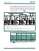
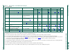
[1] Some legacy Standard-mode devices had fixed input levels of V
IL
= 1.5 V and V
IH
= 3.0 V. Refer to component data sheets.
[2] Maximum V
IH
=V
DD(max)
+ 0.5 V or 5.5 V, which ever is lower. See component data sheets.
[3] The same resistor value to drive 3 mA at 3.0 V V
DD
provides the same RC time constant when using <2 V V
DD
with a smaller current draw.
[4] In order to drive full bus load at 400 kHz, 6 mA I
OL
is required at 0.6 V V
OL
. Parts not meeting this specification can still function, but not at 400 kHz and 400 pF.
[5] The maximum t
f
for the SDA and SCL bus lines quoted in Ta ble 1 0 (300 ns) is longer than the specified maximum t
of
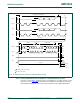
for the output stages (250 ns). This allows series protection
resistors (R
s
) to be connected between the SDA/SCL pins and the SDA/SCL bus lines as shown in Figure 45 without exceeding the maximum specified t
f
.
[6] Necessary to be backwards compatible with Fast-mode.
[7] In Fast-mode Plus, fall time is specified the same for both output stage and bus timing. If series resistors are used, designers should allow for this when considering bus timing.
[8] Input filters on the SDA and SCL inputs suppress noise spikes of less than 50 ns.
[9] If V
DD
is switched off, I/O pins of Fast-mode and Fast-mode Plus devices must not obstruct the SDA and SCL lines.
[10] Special purpose devices such as multiplexers and switches may exceed this capacitance because they connect multiple paths together.
Table 9. Characteristics of the SDA and SCL I/O stages
n/a = not applicable.
Symbol Parameter Conditions Standard-mode Fast-mode Fast-mode Plus Unit
Min Max Min Max Min Max
V
IL
LOW-level input voltage
[1]
−0.5 0.3V
DD
−0.5 0.3V
DD
−0.5 0.3V
DD
V
V
IH
HIGH-level input voltage
[1]
0.7V
DD
[2]
0.7V
DD
[2]
0.7V
DD
[1]
[2]
V
V
hys
hysteresis of Schmitt trigger inputs - - 0.05V
DD
- 0.05V
DD
-V
V
OL1
LOW-level output voltage 1 (open-drain or open-collector)
at 3 mA sink current;
V
DD
>2V
0 0.4 0 0.4 0 0.4 V
V
OL2
LOW-level output voltage 2 (open-drain or open-collector)
at 2 mA sink current
[3]
;
V
DD
≤ 2V
-- 00.2V
DD
00.2V
DD
V
I
OL
LOW-level output current V
OL
=0.4V 3 - 3 - 20 - mA
V
OL
=0.6V
[4]
-- 6 - - -mA
t
of
output fall time from V
IHmin
to V
ILmax
- 250
[5]
20 ×
(V
DD
/5.5V)
[6]
250
[5]
20 ×
(V
DD
/5.5V)
[6]
120
[7]
ns
t
SP
pulse width of spikes that must be
suppressed by the input filter
-- 0 50
[8]
050
[8]
ns
I
i
input current each I/O pin 0.1V
DD
<V
I
< 0.9V
DDmax
−10 +10 −10
[9]
+10
[9]
−10
[9]
+10
[9]
μA
C
i
capacitance for each I/O pin
[10]
-10 - 10 - 10pF