
Data Sheet

UM10204 All information provided in this document is subject to legal disclaimers. © NXP Semiconductors N.V. 2014. All rights reserved.
User manual Rev. 6 — 4 April 2014 37 of 64
NXP Semiconductors
UM10204
I
2
C-bus specification and user manual
5.3 Hs-mode
High-speed mode (Hs-mode) devices offer a quantum leap in I
2
C-bus transfer speeds.
Hs-mode devices can transfer information at bit rates of up to 3.4 Mbit/s, yet they remain
fully downward compatible with Fast-mode Plus, Fast- or Standard-mode (F/S) devices for
bidirectional communication in a mixed-speed bus system. With the exception that
arbitration and clock synchronization is not performed during the Hs-mode transfer, the
same serial bus protocol and data format is maintained as with the F/S-mode system.
5.3.1 High speed transfer
To achieve a bit transfer of up to 3.4 Mbit/s, the following improvements have been made
to the regular I
2
C-bus specification:
• Hs-mode master devices have an open-drain output buffer for the SDAH signal and a
combination of an open-drain pull-down and current-source pull-up circuit on the
SCLH output. This current-source circuit shortens the rise time of the SCLH signal.
Only the current-source of one master is enabled at any one time, and only during
Hs-mode.
• No arbitration or clock synchronization is performed during Hs-mode transfer in
multi-master systems, which speeds-up bit handling capabilities. The arbitration
procedure always finishes after a preceding master code transmission in F/S-mode.
• Hs-mode master devices generate a serial clock signal with a HIGH to LOW ratio of
1 to 2. This relieves the timing requirements for set-up and hold times.
• As an option, Hs-mode master devices can have a built-in bridge. During Hs-mode
transfer, the high-speed data (SDAH) and high-speed serial clock (SCLH) lines of
Hs-mode devices are separated by this bridge from the SDA and SCL lines of
F/S-mode devices. This reduces the capacitive load of the SDAH and SCLH lines
resulting in faster rise and fall times.
• The only difference between Hs-mode slave devices and F/S-mode slave devices is
the speed at which they operate. Hs-mode slaves have open-drain output buffers on
the SCLH and SDAH outputs. Optional pull-down transistors on the SCLH pin can be
used to stretch the LOW level of the SCLH signal, although this is only allowed after
the acknowledge bit in Hs-mode transfers.
• The inputs of Hs-mode devices incorporate spike suppression and a Schmitt trigger at
the SDAH and SCLH inputs.
• The output buffers of Hs-mode devices incorporate slope control of the falling edges
of the SDAH and SCLH signals.
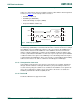
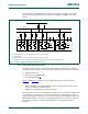
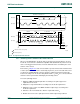
Figure 32
shows the physical I
2
C-bus configuration in a system with only Hs-mode
devices. Pins SDA and SCL on the master devices are only used in mixed-speed bus
systems and are not connected in an Hs-mode only system. In such cases, these pins can
be used for other functions.
Optional series resistors R
s
protect the I/O stages of the I
2
C-bus devices from
high-voltage spikes on the bus lines and minimize ringing and interference.
Pull-up resistors R
p
maintain the SDAH and SCLH lines at a HIGH level when the bus is
free and ensure that the signals are pulled up from a LOW to a HIGH level within the
required rise time. For higher capacitive bus-line loads (>100 pF), the resistor R
p
can be
replaced by external current source pull-ups to meet the rise time requirements. Unless