
Data Sheet


UM10204 All information provided in this document is subject to legal disclaimers. © NXP Semiconductors N.V. 2014. All rights reserved.
User manual Rev. 6 — 4 April 2014 27 of 64
NXP Semiconductors
UM10204
I
2
C-bus specification and user manual
3.2.6 Acknowledge (ACK) and Not Acknowledge (NACK)
Since the slaves are not able to respond the ninth clock cycle, the ACK and NACK are not
required. However, the clock cycle is preserved in the UFm to be compatible with the
I
2
C-bus protocol. The ACK and NACK are also referred to as the ninth clock cycle. The
master generates all clock pulses, including the ninth clock pulse. The ninth data bit is
always driven HIGH (‘1’). Slave devices are not allowed to drive the SDA line at any time.
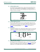
3.2.7 The slave address and R/W bit
Data transfers follow the format shown in Figure 26. After the START condition (S), a
slave address is sent. This address is seven bits long followed by an eighth bit which is a
data direction bit (W
) — a ‘zero’ indicates a transmission (WRITE); a ‘one’ indicates a
request for data (READ) and is not supported by UFm (except for the START byte,
Section 3.2.12
) since the communication is unidirectional (refer to Figure 27). A data
transfer is always terminated by a STOP condition (P) generated by the master. However,
if a master still wishes to communicate on the bus, it can generate a repeated START
condition (Sr) and address another slave without first generating a STOP condition.
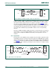
The UFm data transfer format is:
• Master-transmitter transmits to slave-receiver. The transfer direction is not changed
(see Figure 28
). The master never acknowledges because it never receives any data
but generates the ‘1’ on the ninth bit for the slave to conform to the I
2
C-bus protocol.
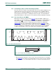
Fig 26. A complete UFm data transfer
S
1 - 7 8 9 1 - 7 8 9 1 - 7 8 9
P
STOP
condition
START
condition
DATA NACKDATA NACKADDRESS NACKW
USDA
USCL
002aag658
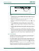
Fig 27. The first byte after the START procedure
002aag659
W
LSBMSB
slave address