
Data Sheet


2
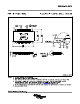
TOT DS(ON) OUT(RMS)
P 4 R I u u
DRV8825
www.ti.com
SLVSA73F –APRIL 2010–REVISED JULY 2014
Thermal Protection (continued)
(5)
where P
TOT
is the total power dissipation, R
DS(ON)
is the resistance of each FET, and I
OUT(RMS)
is the RMS output
current being applied to each winding. I
OUT(RMS)
is equal to the approximately 0.7x the full-scale output current
setting. The factor of 4 comes from the fact that there are two motor windings, and at any instant two FETs are
conducting winding current for each winding (one high-side and one low-side).
The maximum amount of power that can be dissipated in the device is dependent on ambient temperature and
heatsinking.
Note that R
DS(ON)
increases with temperature, so as the device heats, the power dissipation increases. This must
be taken into consideration when sizing the heatsink.
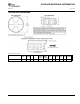
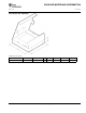
11.3.2 Heatsinking
The PowerPAD™ package uses an exposed pad to remove heat from the device. For proper operation, this pad
must be thermally connected to copper on the PCB to dissipate heat. On a multi-layer PCB with a ground plane,
this can be accomplished by adding a number of vias to connect the thermal pad to the ground plane. On PCBs
without internal planes, copper area can be added on either side of the PCB to dissipate heat. If the copper area
is on the opposite side of the PCB from the device, thermal vias are used to transfer the heat between top and
bottom layers.
For details about how to design the PCB, refer to TI application report SLMA002, "PowerPAD™ Thermally
Enhanced Package" and TI application brief SLMA004, PowerPAD™ Made Easy, available at www.ti.com.
In general, the more copper area that can be provided, the more power can be dissipated. It can be seen that the
heatsink effectiveness increases rapidly to about 20 cm
2
, then levels off somewhat for larger areas.
Copyright © 2010–2014, Texas Instruments Incorporated Submit Documentation Feedback 23
Product Folder Links: DRV8825