
Data Sheet


DRV8825
www.ti.com
SLVSA73F –APRIL 2010–REVISED JULY 2014
8.3.6 nRESET, nENBL, and nSLEEP Operation
The nRESET pin, when driven active low, resets internal logic, and resets the step table to the home position. It
also disables the H-bridge drivers. The STEP input is ignored while nRESET is active.
The nENBL pin is used to control the output drivers and enable/disable operation of the indexer. When nENBL is
low, the output H-bridges are enabled, and rising edges on the STEP pin are recognized. When nENBL is high,
the H-bridges are disabled, the outputs are in a high-impedance state, and the STEP input is ignored.
Driving nSLEEP low will put the device into a low power sleep state. In this state, the H-bridges are disabled, the
gate drive charge pump is stopped, the V3P3OUT regulator is disabled, and all internal clocks are stopped. In
this state all inputs are ignored until nSLEEP returns inactive high. When returning from sleep mode, some time
(approximately 1 ms) needs to pass before applying a STEP input, to allow the internal circuitry to stabilize. Note
that nRESET and nENABL have internal pulldown resistors of approximately 100 kΩ. The nSLEEP pin has an
internal pulldown resistor of 1 MΩ. nSLEEP and nRESET signals need to be driven to logic high for device
operation.
8.3.7 Protection Circuits
The DRV8825 is fully protected against undervoltage, overcurrent, and overtemperature events.
8.3.7.1 Overcurrent Protection (OCP)
An analog current limit circuit on each FET limits the current through the FET by removing the gate drive. If this
analog current limit persists for longer than the OCP time, all FETs in the H-bridge will be disabled and the
nFAULT pin will be driven low. The device remains disabled until either nRESET pin is applied, or VM is
removed and reapplied.
Overcurrent conditions on both high-side and low-side devices; that is, a short to ground, supply, or across the
motor winding all result in an overcurrent shutdown. Note that overcurrent protection does not use the current
sense circuitry used for PWM current control, and is independent of the I
SENSE
resistor value or xVREF voltage.
8.3.7.2 Thermal Shutdown (TSD)
If the die temperature exceeds safe limits, all FETs in the H-bridge will be disabled and the nFAULT pin will be
driven low. After the die temperature has fallen to a safe level, operation automatically resumes.
8.3.7.3 Undervoltage Lockout (UVLO)
If at any time the voltage on the VM pins falls below the UVLO threshold voltage, all circuitry in the device will be
disabled and internal logic will be reset. Operation will resume when V
(VMx)
rises above the UVLO threshold.
8.4 Device Functional Modes
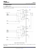
8.4.1 STEP/DIR Interface
The STEP/DIR interface provides a simple method for advancing through the indexer table. For each rising edge
on the STEP pin, the indexer travels to the next state in the table. The direction it moves in the table is
determined by the input to the DIR pin. The signals applied to the STEP and DIR pins should not violate the
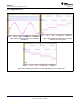
timing diagram specified in Figure 1.
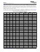
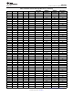
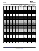
8.4.2 Microstepping
The microstepping indexer allows for a variety of stepping configurations. The state of the indexer is determined
by the configuration of the three MODE pins (refer to Table 1 for configuration options). The DRV8825 supports
full step up to 1/32 microstepping.
Copyright © 2010–2014, Texas Instruments Incorporated Submit Documentation Feedback 17
Product Folder Links: DRV8825