
Data Sheet
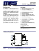

MP6500 – 35V, 2.5A, STEP MOTOR DRIVER W/ INTERNAL CURRENT SENSE
MP6500 Rev. 1.0 www.MonolithicPower.com 3
6/22/2017 MPS Proprietary Information. Patent Protected. Unauthorized Photocopy and Duplication Prohibited.
© 2017 MPS. All Rights Reserved.
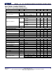
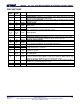
ABSOLUTE MAXIMUM RATINGS
(1)
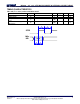
Supply voltage (VIN) ...................... -0.3V to 40V
xOUTx voltage (V
A/BOUT1/2
) .............. -0.7V to 40V
VCP, CPB .............................. VIN to VIN + 6.5V
All other pins to AGND .................. -0.3V to 6.5V
ESD rating (HBD) ........................................ 2kV
Continuous power dissipation (T
A
= +25°C)
(2)
QFN ........................................................... 3.5W
TSSOP ...................................................... 3.9W
Storage temperature ................ -55°C to +150°C
Junction temperature ............................. +150°C
Lead temperature (solder) ..................... +260°C
Recommended Operating Conditions
(3)
Supply voltage (VIN) ....................... 4.5V to 35V
Output current (I
A,BOUT
) .............................. ±2.5A
Operating junction temp. (T
J
). .. -40°C to +125°C
Thermal Resistance
(4)
θ
JA
θ
JC
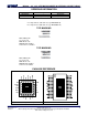
QFN-25 (5mmx5mm) ............ 36 ........ 8 .... °C/W
TSSOP-28 EP ....................... 32 ........ 6 .... °C/W
NOTES:
1) Exceeding these ratings may damage the device.
2) The maximum allowable power dissipation is a function of the
maximum junction temperature T
J
(MAX), the junction-to-
ambient thermal resistance θ
JA
, and the ambient temperature
T
A
. The maximum allowable continuous power dissipation at
any ambient temperature is calculated by P
D
(MAX) = (T
J
(MAX)-T
A
)/θ
JA
. Exceeding the maximum allowable power
dissipation produces an excessive die temperature, causing
the regulator to go into thermal shutdown. Internal thermal
shutdown circuitry protects the device from permanent
damage.
3) The device is not guaranteed to function outside of its operating
conditions.
4) Measured on JESD51-7, 4-layer PCB.