
Data Sheet

DRV8834
www.ti.com
SLVSB19D –FEBRUARY 2012–REVISED MARCH 2015
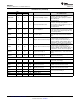
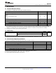
7.5 Electrical Characteristics
T
A
= 25°C, over operating free-air temperature range (unless otherwise noted)
PARAMETER TEST CONDITIONS MIN TYP MAX UNIT
POWER SUPPLY
V
M
= 5 V, excluding winding current 2.4 4
I
VM
VM operating supply current mA
V
M
= 10 V, excluding winding current 2.75
V
M
= 5 V 0.6 2
I
VMQ
VM sleep mode supply current μA
V
M
= 10 V 9.6
V
UVLO
VM undervoltage lockout voltage V
M
falling 2.39 V
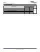
INTERNAL REGULATORS
V
INT
VINT voltage V
M
> 3.3 V, I
OUT
= 0 A to 1 mA 2.85 3 3.15 V
V
REFO
VREF voltage I
OUT
= 0 A to 400 µA 1.9 2 2.1 V
LOGIC-LEVEL INPUTS
nSLEEP 0.5
V
IL
Input low voltage V
All other digital input pins 0.7
nSLEEP 2.5
V
IH
Input high voltage V
All other digital input pins 2
nSLEEP 0.2
V
HYS
Input hysteresis V
All except nSLEEP 0.4
nSLEEP 500
R
PD
Input pulldown resistance kΩ
All except nSLEEP, M0 200
I
IL
Input low current VIN = 0 1 μA
I
IN
Input current (M0) -20 20 µA
VIN = 3.3 V, nSLEEP 6.6 13
I
IH
Input high current μA
VIN = 3.3 V, all except nSLEEP 16.5 33
t
DEG
Input deglitch time 312 468 ns
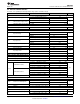
nFAULT OUTPUT (OPEN-DRAIN OUTPUT)
V
OL
Output low voltage I
O
= 5 mA 0.5 V
I
OH
Output high leakage current V
O
= 3.3 V 1 μA
H-BRIDGE FETs
V
M
= 5 V, I
O
= 500 mA, T
J
= 25°C 160 250
V
M
= 5 V, I
O
= 500 mA, T
J
= 85°C 190
HS FET ON-resistance
V
M
= 2.7 V, I
O
= 500 mA, T
J
= 25°C 200 295
V
M
= 2.7 V, I
O
= 500 mA, T
J
= 85°C 240
R
DS(ON)
mΩ
V
M
= 5 V, I
O
= 500 mA, T
J
= 25°C 145 240
V
M
= 5 V, I
O
= 500 mA, T
J
= 85°C 180
LS FET ON-resistance
V
M
= 2.7 V, I
O
= 500 mA, T
J
= 25°C 190 285
V
M
= 2.7 V, I
O
= 500 mA, T
J
= 85°C 235
I
OFF
Off-state leakage current –2 2 μA
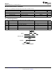
MOTOR DRIVER
f
PWM
Current control PWM frequency Internal PWM frequency 42.5 kHz
V
REF
> 375 mV or DAC codes > 29% 2.4
t
BLANK
Current sense blanking time µs
V
REF
< 375 mV or DAC codes < 29% 1.6
t
R
Rise time V
M
= 5 V, 16 Ω to GND, 10% to 90% V
M
120 ns
t
F
Fall time V
M
= 5 V, 16 Ω to GND, 10% to 90% V
M
100 ns
PROTECTION CIRCUITS
I
OCP
Overcurrent protection trip level 2 A
V
REF
> 375 mV or DAC codes > 29% 1.6
t
OCP
Overcurrent protection period µs
V
REF
< 375 mV or DAC codes < 29% 1.1
Copyright © 2012–2015, Texas Instruments Incorporated Submit Documentation Feedback 7
Product Folder Links: DRV8834