
Data Sheet
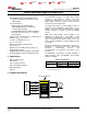

DRV8834
www.ti.com
SLVSB19D –FEBRUARY 2012–REVISED MARCH 2015
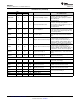
7 Specifications
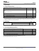
7.1 Absolute Maximum Ratings
over operating free-air temperature range (unless otherwise noted)
(1)(2)
MIN MAX UNIT
VM Power supply voltage –0.3 11.8 V
AVREF,
BVREF,
VINT,
Analog input pin voltage –0.5 3.6 V
ADECAY
,
BDECAY
Digital input pin voltage –0.5 7 V
xISEN pin voltage –0.3 0.5 V
Peak motor drive output current, t < 1 µs Internally limited A
T
J
Operating virtual junction temperature –40 150 °C
T
stg
Storage temperature –60 150 °C
(1) Stresses beyond those listed under absolute maximum ratings may cause permanent damage to the device. These are stress ratings
only, and functional operation of the device at these or any other conditions beyond those indicated under recommended operating
conditions is not implied. Exposure to absolute–maximum–rated conditions for extended periods may affect device reliability.
(2) All voltage values are with respect to network ground terminal.
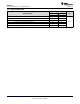
7.2 ESD Ratings
VALUE UNIT
Human body model (HBM), per ANSI/ESDA/JEDEC JS-001, all pins
(1)
±4000
V
(ESD)
Electrostatic discharge V
Charged device model (CDM), per JEDEC specification JESD22-C101, all
±1500
pins
(2)
(1) JEDEC document JEP155 states that 500-V HBM allows safe manufacturing with a standard ESD control process.
(2) JEDEC document JEP157 states that 250-V CDM allows safe manufacturing with a standard ESD control process.
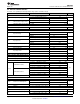
7.3 Recommended Operating Conditions
T
A
= 25°C, over operating free-air temperature range (unless otherwise noted)
MIN NOM MAX UNIT
V
M
Motor power supply voltage range
(1)
2.5 10.8 V
V
REF
VREF input voltage range
(2)
1 2.1 V
I
VINT
VINT external load current 1 mA
I
VREF
VREF external load current 400 µA
V
DIGIN
Digital input pin voltage range –0.3 5.75 V
I
OUT
Continuous RMS or DC output current per bridge
(3)
1.5 A
(1) R
DS(ON)
increases and maximum output current is reduced at VM supply voltages below 5 V.
(2) Operational at VREF between 0 V and 1 V, but accuracy is degraded.
(3) Power dissipation and thermal limits must be observed.
Copyright © 2012–2015, Texas Instruments Incorporated Submit Documentation Feedback 5
Product Folder Links: DRV8834