
Data Sheet


VM
VCP
AOUT1
AOUT2
BOUT1
BOUT2
NFAULT
VINT
AISEN
BISEN
GND
NENBL/AENBL
STEP/BENBL
DIR/BPHASE
M0/APHASE
M1
CONFIG
VREFO
AVREF
BVREF
ADECAY
NSLEEP
BDECAY
VM
Motor A Enable
Motor B Enable
Motor B Direction
Motor A Direction
LOW = SLEEP
VM
10 uf
0.01 uf
2.2 uf
M
M
DRV8834
www.ti.com
SLVSB19D –FEBRUARY 2012–REVISED MARCH 2015
Typical Application (continued)
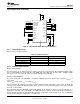
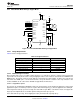
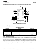
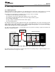
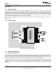
Figure 9. Phase/Enable Mode Driving Two DC Motors
9.2.1.1 Design Requirements
Table 5 lists the design parameters.
Table 5. Design Parameters
PARAMETER REFERENCE EXAMPLE VALUE
Motor voltage VM 10 V
Motor RMS current I
RMS
0.8 A
Motor start-up current I
START
1 A
Motor current trip point I
TRIP
1.5 A
9.2.1.2 Detailed Design Procedure
9.2.1.2.1 Motor Voltage
The motor voltage to use will depend on the ratings of the motor selected and the desired RPM. A higher voltage
spins a brushed DC motor faster with the same PWM duty cycle applied to the power FETs. A higher voltage
also increases the rate of current change through the inductive motor windings.
9.2.1.2.2 Power Dissipation
The power dissipation of the DRV8834 is a function of RMS motor current and the FET resistance (
RDS(ON)
) of
each output.
Power ≈ I
RMS
2
× (High-Side R
DS(ON)
+ Low-Side R
DS(ON)
) (2)
For this example, the ambient temperature is 35°C, and the junction temperature reaches 65°C. At 65°C, the
sum of R
DS(ON)
is about 1 Ω. With an example motor current of 0.8 A, the dissipated power in the form of heat will
be 0.8 A
2
× 1 Ω = 0.64 W.
The temperature that the DRV8834 reaches will depend on the thermal resistance to the air and PCB. It is
important to solder the device PowerPAD to the PCB ground plane, with vias to the top and bottom board layers,
in order dissipate heat into the PCB and reduce the device temperature. In the example used here, the DRV8834
had an effective thermal resistance R
θJA
of 47°C/W, and:
Copyright © 2012–2015, Texas Instruments Incorporated Submit Documentation Feedback 21
Product Folder Links: DRV8834