
Data Sheet

TB67S279FTG
2017-09-15
7
♦Basic function of stepping motor control
1. CLK function
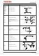
Each up-edge of the CLK signal shifts the current step and electrical angle of the motor.
Note: Analog filter of 200 ns (±20 %) is adopted to CLK pin in the IC
CLK Function
↑ Shifts the electrical angle and current step per each up-edge.
↓ — (no change, maintain former state)
2. ENABLE function
The ENABLE pin controls the ON and OFF of the stepping motor outputs. Motor operation is started by switching ON and
stopped by switching OFF. (In the state of OFF, all of the output MOSFET are turned off and become high impedance state
(Hi-Z).) It is recommended to set the ENABLE pin to Low during VM power-on and power-off sequence to avoid any motor
operation when VM voltage is below the operation range. And so, switching the ENABLE pin to High after VM voltage is
stabilized as the actually used voltage is recommended.
ENABLE Function
High Motor outputs: ON (Normal operation)
Low Motor outputs: OFF (Hi-Z)
3. CW/CCW function / Output pin function (output logic at charge starting)
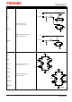
The CW/CCW pin controls the rotation direction of the stepping motor. When CW/CCW is set to High, OUT (+) outputs high
and OUT (-) outputs low in Charge starting. When CW/CCW is set to Low, OUT (+) outputs Low and OUT (-) outputs High
in Charge starting.
CW/CCW Function
High (CW) Clock-wise: The current of Ach leads the current of Bch by 90-degree phase difference.
Low (CCW) Counter clock-wise: The current of Bch leads the current of Ach by 90-degree phase difference.
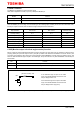
4. DMODE (step resolution setting) function
The DMODE pins are used to set the step resolution for stepping motor operation. If all 3 pins (DMODE0, 1, and 2) are set
to Low, the device goes into ‘standby mode’. During ‘standby mode’, few internal circuits are fully shutdown to reduce power
dissipation. If any of the 3 pins (DMODE0, 1, or 2) is set to High, the TB67S279FTG will reboot from standby mode.
However, it will take 7.5 μs (typ.) to stabilize the internal circuit. Therefore, please wait for this warm-up period and input
signals to boot up.
Note: Built-in digital filter of 1.25 μs (±20 %) is adopted to DMODE pins.
Note: Built-in digital filter of 0.94 μs (±20 %) is adopted to DMODE pins for standby mode.
DMODE0 DMODE1 DMODE2 Function
High High High 1/32 step resolution
High
High Low 1/16 step resolution
High
Low High 1/8 step resolution
High
Low Low 1/2 (b) step resolution
Low
High High 1/4 step resolution
Low
High Low 1/2 (a) step resolution
Low
Low High 1/1 step resolution
Low Low Low
Standby mode
(Internal oscillator circuit (OSCM) and output MOSFETs are set to ‘OFF’)
DMODE0, 1, and 2 pins can be switched during operation. For the following step, the current of the nearest electric angle
before or after switching will flow. Please refer to the application note for detailed functions.