
Data Sheet

TB67S279FTG
2017-09-15
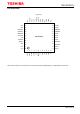
4
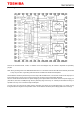
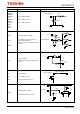
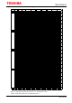
Block diagram
Some of the functional blocks, circuits, or constants in the block diagram may be omitted or simplified for explanatory
purpose.
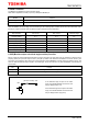
Note: All the grounding wires of the TB67S279FTG should run on the solder mask on the PCB and be externally terminated
at only one point. Also, a grounding method should be considered for efficient heat dissipation.
Careful attention should be paid to the layout of the output, VM and GND traces, to avoid short circuits across output pins or
to the power supply or ground. If such a short circuit occurs, the device may be permanently damaged.
Also, the utmost care should be taken for pattern designing and implementation of the device since it has power supply pins
(VM, RS line, OUT line, and GND) through which a particularly large current may run. If these pins are wired incorrectly, an
operation error may occur or the device may be destroyed.
The logic input pins must also be wired correctly. Otherwise, the device may be damaged owing to a current running
through the IC that is larger than the specified current. Careful attention should be paid to design patterns and mountings.