
Data Sheet

TB67S279FTG
2017-09-15
20
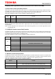
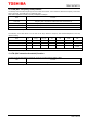
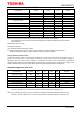
Electrical characteristics 1 (Ta = 25°C and VM = 24 V, unless otherwise specified)
Characteristics Symbol Test condition Min Typ. Max Unit
Logic input voltage 1
(Except BOOST, CLIM1, and FLIM)
VIN1 (H)
High level
2.0
—
5.5
V
VIN1 (L)
Low level
0
—
0.8
V
Logic input hysteresis voltage
VIN (HYS)
Hysteresis voltage
0.1
—
0.3
V
Logic input voltage 2
(BOOST, CLIM1, and FLIM)
VIN2 (H)
VCC short
4.2
—
VCC
V
VIN2 (PU)
VCC-100 kΩ pull-up
2.8
—
3.55
V
VIN2 (PD)
GND-100 kΩ pull-down
1.45
—
2.2
V
VIN2 (L)
GND short
0
—
0.8
V
Logic input current 1
(Except BOOST, CLIM1, and FLIM)
IIN1 (H)
Input voltage=3.3 V
—
33
—
µA
IIN1 (L)
Input voltage=0 V
—
—
1
µA
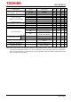
MO output pin voltage
VOL (MO)
IOL=5 mA LO=Low
—
0.2
0.5
V
LO output pin voltage
VOL (LO)
IOL=5 mA LO=Low
—
0.2
0.5
V
Current consumption
IM1
Standby mode
—
2
—
mA
IM2
OUT: OPEN, ENABLE: Low,
Standby mode: Release
3 5 7 mA
IM3
OUT: OPEN, ENABLE: High,
Standby mode: Release
4 6 8 mA
Output leakage current
High-side
IOH VM=50 V,VOUT=0 V — — 1 µA
Low-side
IOL
VM=VOUT=50 V
1
—
—
µA
Motor current channel differential ΔIOUT1
Current differential between
channels
-5 0 5 %
Motor current setting differential
ΔIOUT2
IOUT=1.0 A
-5
0
5
%
Motor output ON-resistance
( High-side + Low-side)
Ron (H+L)
Tj=25°C, Forward direction
(High + Low side)
— 0.6 0.75
Ω
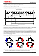
Note: VIN (H) is defined as the VIN voltage that causes the outputs (OUTA+, OUTA-, OUTB+ and OUTB-) to change when
a pin under test is gradually raised from 0 V. VIN (L) is defined as the VIN voltage that causes the outputs (OUTA+,
OUTA-, OUTB+ and OUTB-) to change when the pin is then gradually lowered. The difference between VIN (H) and
VIN (L) is defined as the VIN (HYS).