
Data Sheet

TB67S279FTG
2017-09-15
19
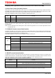
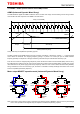
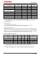
Absolute maximum ratings (Ta = 25°C)
Characteristics
Symbol Rating Unit Remarks
Motor power supply
VM
50
V
—
Motor output voltage
VOUT
50
V
—
Motor output current
IOUT
2.0
A
(Note1)
Internal Logic power supply
VCC
6.0
V
—
Logic input voltage
VIN (H)
6.0
V
—
VIN (L)
-0.4
V
—
MO output voltage
VMO
6.0
V
—
LO output voltage
VLO
6.0
V
—
MO Inflow current
IMO
6.0
mA
—
LO Inflow current
ILO
6.0
mA
—
Power dissipation
PD
1.3
W
(Note2)
Operating temperature
Topr
-20 to 85
°C
—
Storage temperature
Tstg
-55 to 150
°C
—
Junction temperature
Tj (max)
150
°C
—
Note1: For normal usage, the maximum current value should be determined by heat calculation.
The maximum output current may be further limited depending on ambient temperature and board conditions
(heat conditions).
Note2: Device alone (Ta =25°C)
Ta: Ambient temperature
Topr: Ambient temperature while the IC is active
Tj: Junction temperature while the IC is active. Tj (max) is limited by the thermal shutdown (TSD) threshold.
Please set the usage conditions so that the peak Tj is kept under 120°C for indication.
Caution) Absolute maximum ratings
The absolute maximum ratings of a semiconductor device are a set of ratings that must not be exceeded, even for a
moment. Do not exceed any of these ratings. Exceeding the rating (s) may cause device breakdown, damage or
deterioration, and may result in injury by explosion or combustion. The value of even one parameter of the absolute
maximum ratings should not be exceeded under any circumstances. All voltage ratings, including supply voltages, must
always be followed. Other notes and considerations described in the datasheet should also be referred to.
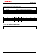
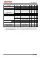
Operation ranges
(Ta=-20 to 85
°C
)
Characteristics Symbol
Min Typ. Max Unit Remarks
Motor power supply
VM
10
24
47
V
—
Motor output current
IOUT
—
1.0
2.0
A
(Note1)
MO output pin voltage
VMO
—
3.3
VCC
V
Pull-up voltage
LO output pin voltage
VLO
—
3.3
VCC
V
Pull-up voltage
Clock input frequency
fCLK
—
-—
1000
kHz
(Note2)
Chopping frequency
Fchop (range)
40
70
150
kHz
—
VREF input voltage
VREF
GND
2.0
3.6
V
—
Note1: The actual maximum current may be limited due to operating circumstances (operating conditions of step resolution,
continuous operation time, etc. and thermal conditions of ambient temperature, PCB layout, etc.)
Note2: The actual maximum frequency may be limited due to operating circumstances (operating conditions of step
resolution, continuous operation time, etc. and thermal conditions of ambient temperature, PCB layout, etc.)