
Data Sheet


TB67S249FTG
2017-08-18
3
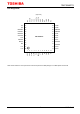
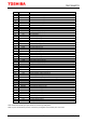
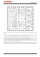
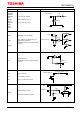
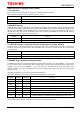
Pin description
Pin No
Pin name
Pin function
1
AGC0
Active Gain Control setup pin No.0
2
AGC1
Active Gain Control setup pin No.1
3
CLIM0
AGC current limiter setup pin No.0
4
CLIM1
AGC current limiter setup pin No.1
5
FLIM
AGC frequency limiter setup pin
6
BOOST
AGC current boost setup pin
7
LTH
AGC threshold setup pin
8
GND
Ground pin
9
NC
Non connection
10
VMA
Motor power supply input pin
11
VMA
Motor power supply input pin
12
NC
Non connection
13
OUTA+
Ach motor output (+) pin
14
OUTA+
Ach motor output (+) pin
15
RSAGND
Ach motor power ground pin
16
RSAGND
Ach motor power ground pin
17
OUTA-
Ach motor output (-) pin
18
OUTA-
Ach motor output (-) pin
19
OUTB-
Bch motor output (-) pin
20
OUTB-
Bch motor output (-) pin
21
RSBGND
Bch motor power ground pin
22
RSBGND
Bch motor power ground pin
23
OUTB+
Bch motor output (+) pin
24
OUTB+
Bch motor output (+) pin
25
NC
Non connection
26
VMB
Motor power supply input pin
27
VMB
Motor power supply input pin
28
NC
Non connection
29
GND
Ground pin
30
GND
Ground pin
31
VREFB
Bch current threshold reference pin
32
VREFA
Ach current threshold reference pin
33
VCC
Internal regulator voltage monitor pin
34
VCC
Internal regulator voltage monitor pin
35
OSCM
Internal oscillator frequency monitor and setting pin
36
NC
Non connection
37
NC
Non connection
38
NC
Non connection
39
DMODE0
Step resolution setting pin No.0
40
DMODE1
Step resolution setting pin No.1
41
DMODE2
Step resolution setting pin No.2
42
CW/CCW
Current direction setup pin
43
CLK
Step clock input pin
44
ENABLE
Motor output ON/OFF pin
45
RESET
Electrical angle initialize pin
46
MO
Electrical angle monitor pin
47
LO1
Error flag output pin No.1
48
LO2
Error flag output pin No.2
Note: Please leave the NC pins open and do not connect any PCB pattern.
Note: For pins with the same pin name; connect the pins together at the nearest point of the driver.