
Data Sheet

TB67S279FTG, TB67S289FTG, TB67S249FTG Application Note
2018-03-07
4 / 33
Preliminary
4. Output Current
Output current value for the motor depends on the power consumption that refers to the voltage drop
at the on resistance of the output circuit. From the above, the absolute maximum current rating of
each IC is as follows; 2 A (TB67S279FTG), 3 A (TB67S289FTG), and 4.5 A (TBS249FTG). These
ratings must not be exceeded, even for a moment.
The actual-usage maximum current is limited depending on the usage conditions (the ambient
temperature, the wiring pattern of the board, the radiation path, the exciting design, etc.). Therefore,
configure the most appropriate current value after calculating the heat and evaluating the board
under the operating environment.
Moreover, the IC drives the motor with a constant-current control by ACDS technology.
Recommended lower current limit for appropriate motor operation is as follows; TB67S279FTG: 0.5
to 1.0 A, TB67S289FTG: 1.0 to 1.5 A, and TB67S249FTG: 1.5 to 2.0 A. When the configured current
is too small in using large-current drive devices, malfunctions such as offset may occur.
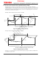
5. Control Logic Input
The IC can avoid malfunction occurred by the electromotive force, which generates when the control
logic signal is input without VM voltage.
However, it is recommended to set the control logic signal low level while VM is not supplied.
Configure the control logic signal low level during powering on and shutdown (refer to “2.1 Power
supply voltage and operation range”) and input the operation signal after VM and VREF reach the
operation voltage range.
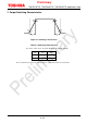
6. PWM Control
6.1. Setting PWM threshold
TB67S279FTG, TB67S289FTG, and TB67S249FTG can configure the constant current PWM
threshold only by the applied voltage to the VREF pin. External current detection resistor is not
required. (ACDS technology)
The current value (Iout) of TB67S279FTG, TB67S289FTG, and TB67S249FTG can be
approximated from below formulas.
Iout = VREF × 0.556 (TB67S279FTG)
Iout = VREF × 0.833 (TB67S289FTG)
Iout = VREF × 1.250 (TB67S249FTG)
VREF gain of each IC is as follows;
TB67S279FTG: 0.556 (typ.)
TB67S289FTG: 0.833 (typ.)
TB67S249FTG: 1.25 (typ.)
Then, when the voltage of 2 V is input to VREF pin in using TB67S289FTG, setting current is as
follows;
Iout = 2 V × 0.833 = 1.67 A (typ.)