Preliminary TB67S279FTG, TB67S289FTG, TB67S249FTG Application Note TB67S279FTG TB67S289FTG TB67S249FTG Usage considerations Main Specifications Product number TB67S279FTG / TB67S289FTG / TB67S249FTG Control I/F CLOCK-IN Absolute maximum ratings 50 V, 2 A (TB67S279FTG), 3 A (TB67S289FTG), 4.
Preliminary TB67S279FTG, TB67S289FTG, TB67S249FTG Application Note 1. Outline of IC TB67S279FTG, TB67S289FTG, and TB67S249FTG can control a single 2-phase bipolar stepping motor. This IC supports from 12 V to 42 V power supply and large-current drive for motors by adopting 50 V monolithic analog process (BiCD: Bipolar CMOS DMOS).
Preliminary TB67S279FTG, TB67S289FTG, TB67S249FTG Application Note 3. Power Supply Sequence There are no special procedures between power sources in powering on and shutdown because TB67S279FTG, TB67S289FTG, and TB67S249FTG can operate with a single power supply by the VCC regulator. Moreover, built-in under voltage detections (UVLO and power on reset function (POR)) avoid malfunction, which occurs at the UVLO/POR detection threshold or less. While POR is activated, the internal logic is initialized.
Preliminary TB67S279FTG, TB67S289FTG, TB67S249FTG Application Note 4. Output Current Output current value for the motor depends on the power consumption that refers to the voltage drop at the on resistance of the output circuit. From the above, the absolute maximum current rating of each IC is as follows; 2 A (TB67S279FTG), 3 A (TB67S289FTG), and 4.5 A (TBS249FTG). These ratings must not be exceeded, even for a moment.
Preliminary TB67S279FTG, TB67S289FTG, TB67S249FTG Application Note 6.2. Setting internal oscillation frequency (fOSCM) and constant current PWM (chopping) frequency (fchop) TB67S279FTG, TB67S289FTG, and TB67S249FTG can set the internal oscillation frequency (fOSCM) and the PWM (chopping) frequency (fchop) with the constant numbers of the external components (resistor and capacitor), which are connected to OSCM pin.
Preliminary TB67S279FTG, TB67S289FTG, TB67S249FTG Application Note 6.2.1. Function of internal oscillation circuit: Elimination of external components The internal oscillation circuit of TB67S279FTG, TB67S289FTG, and TB67S249FTG has the function of eliminating external components. As mentioned previously, the oscillation frequency can be changed arbitrarily by connecting external components (resistor and capacitor) to the OSCM pin and adjusting their constant numbers.
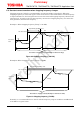
Preliminary TB67S279FTG, TB67S289FTG, TB67S249FTG Application Note 6.3. Constant current waveform when chopping frequency changes Chopping frequency (fchop) is recommended to set about 67 kHz in using the IC. When the chopping frequency is increased, ripple current of the motor is decreased and the waveform quality is improved. However, the heat generates because the increased chopping frequency enhances the switching loss. To improve the waveform quality, increase the chopping frequency.
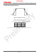
Preliminary TB67S279FTG, TB67S289FTG, TB67S249FTG Application Note 7. Output Switching Characteristics 90% 90% 10% 10% tr tf Figure 7.1 Switching characteristics Table 7.1 Switching characteristics Ta = 25°C, VM = 24 V, No load (Example of TB67S249FTG) Item Typ. Unit tr 80 ns tf 90 ns Note: Confirm the electrical characteristics of the data sheet for each value.
Preliminary TB67S279FTG, TB67S289FTG, TB67S249FTG Application Note 8. Function Explanation This chapter describes the basic functions of stepping motors. 8.1. CLK function An electrical angle advances one unit according to the driving mode, which is configured by each pulse of CLK signal. Each signal is reflected at upper edge of CLK signal. The analog filter of 200 ns (±20%) is implemented for CLK pin to avoid malfunction due to noise. Duty of CLK signal is not necessary to set 50 %.
Preliminary TB67S279FTG, TB67S289FTG, TB67S249FTG Application Note 8.4. RESET function This function initializes the internal electrical angle. The standby mode can be configured by setting DMODE0, DMODE1, and DMODE2 pins low level. Note: Built-in digital filter of 0.625 μs (±20 %) is adopted to RESET pin.
Preliminary TB67S279FTG, TB67S289FTG, TB67S249FTG Application Note 8.5. MO (Monitor Output: electrical angle output) function MO pin outputs an internal initial electrical angle as a signal. Since MO pin is an open drain type pin, please pull up this pin to the power supply such as VCC to enable this function. (The pull-up resistor value should be set between 10 kΩ and 100 kΩ.) MO pin outputs high level with the pulled-up state because it is in high impedance (Hi-Z) state during the normal operation.
Preliminary TB67S279FTG, TB67S289FTG, TB67S249FTG Application Note 8.6. AGC (Active Gain Control) AGC is an abbreviation for Active Gain Control that is our original driving technology. When required motor torque is lower than the configured constant current value, the motor can drive efficiently by decreasing driving current. When higher torque is required, motor stall can be prevented by increasing the constant current value. 8.6.1.
Preliminary TB67S279FTG, TB67S289FTG, TB67S249FTG Application Note 8.6.2. CLIM (AGC bottom current limit) function AGC judges the required torque value and decreases the current value from the constant current, which is set by VREF. In order to avoid stalls including motor-system stalls, this constant current value should have enough margins.
Preliminary TB67S279FTG, TB67S289FTG, TB67S249FTG Application Note 8.6.3. BOOST (current boost) function BOOST pin sets the current boost level (i.e., return to the initial constant current setting value) when the load torque increases. BOOST pin is a 4 stated logic input pin, setting the compensation value in accordance with the existence of the 100 kΩ-resistor. In the following table, Mode 1 has the fastest current recovery, and Mode 4 has the slowest one.
Preliminary TB67S279FTG, TB67S289FTG, TB67S249FTG Application Note 8.6.4. FLIM (AGC frequency limit) function FLIM pin sets the bottom frequency (frequency limit) for AGC to be active. Since AGC uses an induced voltage in operating, some motors have unstable AGC operation when the motor rotation is very slow. Also, the motor’s own resonance frequency influences on the AGC operation. Thereby, the lower frequency limit for AGC activation is necessary to avoid above and can be set by FLIM pin.
Preliminary TB67S279FTG, TB67S289FTG, TB67S249FTG Application Note 9. IC Signal Output Function 9.1. LO1, LO2 (Error Output: Error detect flag output) function LO1 pin and LO2 pin output signals when the error state of the IC or its environment is detected. Both pins are open drain type like MO pin, therefore to use the function properly, they should be pulled up to the power supply (3.3 V/5 V) such as VCC. Use the pull-up resistor in the range of 10 kΩ to 100 kΩ.
Preliminary TB67S279FTG, TB67S289FTG, TB67S249FTG Application Note 10. Application Circuit Example Note: Some of the functional blocks, circuits, or constants in the block diagram may be omitted or simplified for explanatory purposes. Note: Above application circuit example is provided for reference purposes only, and is not guaranteed for mass production. Figure 10.
Preliminary TB67S279FTG, TB67S289FTG, TB67S249FTG Application Note 11. External Component Description 11.1. Capacitors for power supply pins To stabilize the power supply voltage of the IC and reduce the noise, connect an appropriate capacitor to each pin. It is effective and recommended to connect capacitors as close to the IC as possible. However, be sure to consider the influence of the IC’s heat generation.
Preliminary TB67S279FTG, TB67S289FTG, TB67S249FTG Application Note 11.2. Internal oscillation frequency OSCM oscillation frequency can be adjusted by changing the constant numbers of external capacitor and resistor. In adjusting, it is recommended to change the resistor, while fixing the capacitor to 270 pF. Chopping frequency can be also changed by adjusting OSCM frequency. Please refer to below table in adjusting the chopping frequency.
Preliminary TB67S279FTG, TB67S289FTG, TB67S249FTG Application Note Graph of ROSC and fOSCM (reference data/measurement data example) 3.0 2.63 2.5 2.37 2.23 2.08 fOSCM [MHz] 2.0 1.80 1.67 1.55 1.5 1.34 1.15 1.07 0.98 1.0 0.83 0.70 0.58 0.5 0.0 0.0 2.0 4.0 6.0 8.0 10.0 12.0 ROSC [kΩ] Figure 11.1 Graph of ROSC and fOSCM (reference data/measurement data example) Graph of ROSC and fchop (reference data/measurement data example) 180 164.38 160 148.13 139.38 140 130.
Preliminary TB67S279FTG, TB67S289FTG, TB67S249FTG Application Note 11.3. Resistor for monitor pin The IC has MO, LO1, and LO2 open-drain type pins to output some of the internal status of the IC. When internal open-drain MOSFETs turn off, these pins show high impedance. In using this function, they should be pulled up to the power supply (3.3 V/5 V) such as VCC. If this function is not used, leave the pins open or connect them to GND. Table 11.
Preliminary TB67S279FTG, TB67S289FTG, TB67S249FTG Application Note 11.6. Error detection function This IC incorporates a thermal shutdown circuit (TSD) and an over current protection (ISD), which are unique error detections to power ICs, in addition to a general UVLO function. Each function is described below. 11.6.1. Thermal shutdown circuit (TSD) When the junction temperature of the IC reaches a preset specified value, the internal detection circuit operates to turn off the output block.
Preliminary TB67S279FTG, TB67S289FTG, TB67S249FTG Application Note 12. Power Consumption of the IC Power of the IC is consumed mainly by the transistor of the output block and by the internal circuit, which includes the logic block.
Preliminary TB67S279FTG, TB67S289FTG, TB67S249FTG Application Note 13. Power dissipation Relation equation of the ambient temperature (Ta), the junction temperature (Tj), and the heat resistance (Rth(j-a)) between the junction temperature and the ambient temperature is as follows; Tj = Ta + P × Rth(j-a) The IC adopts a surface mounting package, QFN48. QFN48 package radiates the heat mainly from the heat sink of the IC back side to the mounting board.
Preliminary TB67S279FTG, TB67S289FTG, TB67S249FTG Application Note 14. Foot Pattern Example QFN48 foot pattern example (unit: mm) Figure 14.1 QFN48 foot pattern example Note: The data is for reference only and not guaranteed for mass production. In designing the size of mounting board, determine the foot pattern by considering the solder bridge, the solder connecting strength, the pattern accuracy in making board, and the mounting accuracy of the IC board.
Preliminary TB67S279FTG, TB67S289FTG, TB67S249FTG Application Note 15. Board dimensions (original board examples of our company) 15.1. Input/Output DMODE2 DMODE1 DMODE0 VREFA VREFB CW/CCW Apply power supply voltage (VM) CLK ENABLE Short-circuit to SR4 RESET Connect stepping motor MO LO1 LO2 AGC0 AGC1 CLIM0 CLIM1 FLIM BOOST LTH Figure 15.1 Input /Output As for each power supply and control signal, refer to above figure.
Preliminary TB67S279FTG, TB67S289FTG, TB67S249FTG Application Note 15.2. Main part Bypass capacitor for VCC Bypass capacitor for VM Decoupling capacitor for VM Resistor and capacitor for OSCM Pull up resistor for MO Pull up resistor for LO1 Pull up resistor for LO2 Resistor for CLIM1 adjustment Resistor for FLIM adjustment Resistor for BOOST adjustment Resistor for LTH adjustment Figure 15.2 Main part Connect each external components referring to ’10. Application Circuit Example’.
Preliminary TB67S279FTG, TB67S289FTG, TB67S249FTG Application Note 15.3. Options When VCC is used as the switch for high level or as the connecting point for pulled up resistor, short-circuit SR3. In this case, do not apply voltage to VDD pin. Use it when VREF is applied by dividing resistive voltage of VCC. (Refer to the following section of ‘SVF pin’.) When VDD (external power supply) is used as the switch for high level or as the connecting point for pulled up resistor, apply 3.3 V or 5 V to VDD pin.
Preliminary TB67S279FTG, TB67S289FTG, TB67S249FTG Application Note 15.4. Board circuit diagram Figure 15.
Preliminary TB67S279FTG, TB67S289FTG, TB67S249FTG Application Note 15.5. SVF pin The motor current and the torque can be changed during operation by using our optional pattern on the board. (Please refer to below circuit diagram.) The applied voltage for VREF can be adjusted by switching the voltage-dividing ratio with the transistor. Use an appropriate resistor for the SVF input (i.e., the base of the transistor) in accordance with the capability of the transistor.
Preliminary TB67S279FTG, TB67S289FTG, TB67S249FTG Application Note Notes on Contents 1. Block Diagrams Some of the functional blocks, circuits, or constants in the block diagram may be omitted or simplified for explanatory purposes. 2. Equivalent Circuits The equivalent circuit diagrams may be simplified or some parts of them may be omitted for explanatory purposes. 3. Timing Charts Timing charts may be simplified for explanatory purposes. 4.
Preliminary TB67S279FTG, TB67S289FTG, TB67S249FTG Application Note (5) Carefully select external components (such as inputs and negative feedback capacitors) and load components (such as speakers), for example, power amp and regulator. If there is a large amount of leakage current such as from input or negative feedback condenser, the IC output DC voltage will increase. If this output voltage is connected to a speaker with low input withstand voltage, over current or IC failure may cause smoke or ignition.
Preliminary TB67S279FTG, TB67S289FTG, TB67S249FTG Application Note RESTRICTIONS ON PRODUCT USE Toshiba Corporation and its subsidiaries and affiliates are collectively referred to as “TOSHIBA”. Hardware, software and systems described in this document are collectively referred to as “Product”. • TOSHIBA reserves the right to make changes to the information in this document and related Product without notice.