
Data Sheet
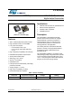
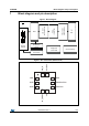

Block diagram and pin description LPS25HB
8/50 DocID027112 Rev 4
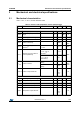
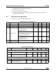
Table 2. Pin description
Pin number Name Function
1 Vdd_IO Power supply for I/O pins
2
SCL
SPC
I²C serial clock (SCL)
SPI serial port clock (SPC)
3 Reserved Connect to GND
4
SDA
SDI
SDI/SDO
I²C serial data (SDA)
4-wire SPI serial data input (SDI)
3-wire serial data input /output (SDI/SDO)
5
SDO
SA0
4-wire SPI serial data output (SDO)
I²C less significant bit of the device address (SA0)
6CS
SPI enable
I²C/SPI mode selection
(1: SPI idle mode / I
2
C communication enabled;
0: SPI communication mode / I
2
C disabled)
7 INT_DRDY Interrupt or Data Ready
8 GND 0 V supply
9 GND 0 V supply
10 VDD Power supply