
Data Sheet

DocID027112 Rev 4 29/50
LPS25HB Digital interfaces
50
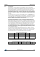
6.3.2 SPI write
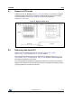
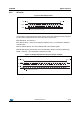
Figure 16.
SPI write protocol
The SPI write command is performed with 16 clock pulses. The multiple byte write command
is performed by adding blocks of 8 clock pulses to the previous one.
bit 0: WRITE bit. The value is 0.
bit 1: MS bit. When 0, does not increment the address; when 1, increments the address in
multiple writes.
bit 2 -7: address AD(5:0). This is the address field of the indexed register.
bit 8-15: data DI(7:0) (write mode). This is the data that is written in the device (MSb first).
bit 16-...: data DI(...-8). Further data in multiple byte writes.
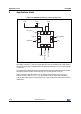
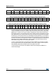
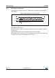
Figure 17.
Multiple byte SPI write protocol (2-byte
example)
CS
SPC
SDI
RW
DI7DI6DI5DI4DI3DI2DI1DI0
AD5 AD4 AD3 AD2 AD1 AD0
AD6
CS
SPC
SDI
RW
AD5 AD4 AD3 AD2 AD1 AD0
DI7 DI6 DI5 DI4 DI3 DI2 DI1 DI0 DI15 DI14 DI13 DI12 DI11 DI10 DI9 DI8
MS