
Data Sheet

Digital interfaces LPS25HB
24/50 DocID027112 Rev 4
6 Digital interfaces
6.1 I
2
C serial interface
The registers embedded in the LPS25HB may be accessed through both the I²C and SPI
serial interfaces. The latter may be SW configured to operate either in 3-wire or 4-wire
interface mode.
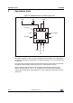
The serial interfaces are mapped onto the same pads. To select/exploit the I²C interface, the
CS
line must be tied high (i.e. connected to Vdd_IO);
to select the SPI interface, the CS line
must be tied low (i.e. connected to GND).
6.2 I
2
C serial interface (CS = High)
The LPS25HB I²C is a bus slave. The I²C is employed to write data into registers whose
content can also be read back.
The relevant I²C terminology is given in Ta b l e 9
.
There are two signals associated with the I²C bus: the serial clock line (SCL) and the serial
data line (SDA). The latter is a bi-directional line used for sending and receiving the data
to/from the interface. Both lines have to be connected to Vdd_IO through pull-up resistors.
The I²C interface is compliant with fast mode (400 kHz) I²C standards as well as with the
normal mode.
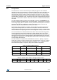
Table 10. Serial interface pin description
Pin name Pin
CS
SPI enable
I²C/SPI mode selection (1: I²C mode; 0: SPI enabled
SCL/SPC
I²C serial clock (SCL)
SPI serial port clock (SPC)
SDA
SDI
SDI/SDO
I²C serial data (SDA)
4-wire SPI serial data input (SDI)
3-wire serial data input /output (SDI/SDO)
SDO
SAO
SPI serial data output (SDO)
I²C less significant bit of the device address (SA0)
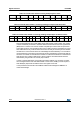
Table 11.
I
2
C terminology
Term Description
Transmitter The device which sends data to the bus
Receiver The device which receives data from the bus
Master The device which initiates a transfer, generates clock signals and terminates a transfer
Slave The device addressed by the master