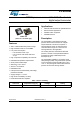
LPS25HB MEMS pressure sensor: 260-1260 hPa absolute digital output barometer Datasheet - production data Applications HLGA-10L (2.5 x 2.5 x 0.76 mm typ.) Altimeter and barometer for portable devices Enhanced GPS applications Weather station equipment Wearable devices Description Features 260 to 1260 hPa absolute pressure range High-resolution mode: 0.01 hPa RMS Low power consumption – Low-resolution mode: 4 μA – Low current & noise mode with FIFO: 4.
Contents LPS25HB Contents 1 Block diagram and pin description . . . . . . . . . . . . . . . . . . . . . . . . . . . . . 7 2 Mechanical and electrical specifications . . . . . . . . . . . . . . . . . . . . . . . . 9 2.1 Mechanical characteristics . . . . . . . . . . . . . . . . . . . . . . . . . . . . . . . . . . . . . 9 2.2 Electrical characteristics . . . . . . . . . . . . . . . . . . . . . . . . . . . . . . . . . . . . . . 10 2.3 Communication interface characteristics . . . . . . . . . . . . .
LPS25HB Contents 6.3 SPI bus interface . . . . . . . . . . . . . . . . . . . . . . . . . . . . . . . . . . . . . . . . . . . 27 6.3.1 SPI read . . . . . . . . . . . . . . . . . . . . . . . . . . . . . . . . . . . . . . . . . . . . . . . . . 28 6.3.2 SPI write . . . . . . . . . . . . . . . . . . . . . . . . . . . . . . . . . . . . . . . . . . . . . . . . 29 6.3.3 SPI read in 3-wire mode . . . . . . . . . . . . . . . . . . . . . . . . . . . . . . . . . . . . 30 7 Register mapping . . . . . . . . . .
Contents 10 4/50 LPS25HB Revision history . . . . . . . . . . . . . . . . . . . . . . . . . . . . . . . . . . . . . . . . . . .
LPS25HB List of tables List of tables Table 1. Table 2. Table 3. Table 4. Table 5. Table 6. Table 7. Table 8. Table 9. Table 10. Table 11. Table 12. Table 13. Table 14. Table 15. Table 16. Table 17. Table 18. Table 19. Table 20. Table 21. Table 22. Table 23. Table 24. Table 25. Table 26. Device summary . . . . . . . . . . . . . . . . . . . . . . . . . . . . . . . . . . . . . . . . . . . . . . . . . . . . . . . . . . 1 Pin description . . . . . . . . . . . . . . . . . . . . . . . . . . . . . . . . . . . .
List of figures LPS25HB List of figures Figure 1. Figure 2. Figure 3. Figure 4. Figure 5. Figure 6. Figure 7. Figure 8. Figure 9. Figure 10. Figure 11. Figure 12. Figure 13. Figure 14. Figure 15. Figure 16. Figure 17. Figure 18. Figure 19. Figure 20. Figure 21. Figure 22. Figure 23. Figure 24. Figure 25. 6/50 Block diagram . . . . . . . . . . . . . . . . . . . . . . . . . . . . . . . . . . . . . . . . . . . . . . . . . . . . . . . . . . . . 7 Pin connections (bottom view) . . . . . . . . . . . . . . . .
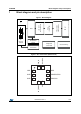
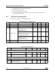
LPS25HB Block diagram and pin description Figure 1. Block diagram I2C SPI Temperature sensor Voltage and current bias Clock and timing Sensor bias SCL/SPC Figure 2.
Block diagram and pin description LPS25HB Table 2.
LPS25HB Mechanical and electrical specifications 2 Mechanical and electrical specifications 2.1 Mechanical characteristics VDD = 1.8 V, T = 25 °C, unless otherwise noted. Table 3. Pressure and temperature sensor characteristics Symbol Parameter Test condition Min. Typ.(1) Max.
Mechanical and electrical specifications LPS25HB 2. Characterization data. Parameter not tested at final test. 3. Embedded quadratic compensation. 4. OPC: One Point Calibration in the application. 5. Pressure noise RMS evaluated in a controlled environment based on the average standard deviation of 32 measurements at highest ODR. 2.2 Electrical characteristics VDD = 1.8 V, T = 25 °C, unless otherwise noted. Table 4. Electrical characteristics Symbol VDD Parameter Test condition Min.
LPS25HB Mechanical and electrical specifications 2.3 Communication interface characteristics 2.3.1 SPI - serial peripheral interface Subject to general operating conditions for Vdd and TOP. Table 6.
Mechanical and electrical specifications LPS25HB I2C - inter-IC control interface 2.3.2 Subject to general operating conditions for Vdd and TOP. Table 7. I2C slave timing values I²C fast mode(1) I²C standard Symbol Parameter (1) f(SCL) SCL clock frequency Min Max Min Max Unit 0 100 0 400 kHz tw(SCLL) SCL clock low time 4.7 1.3 tw(SCLH) SCL clock high time 4.0 0.6 tsu(SDA) SDA setup time 250 100 th(SDA) SDA data hold time 0.01 tr(SDA) tr(SCL) μs ns 3.45 0 0.
LPS25HB 2.4 Mechanical and electrical specifications Absolute maximum ratings Stress above those listed as “Absolute maximum ratings” may cause permanent damage to the device. This is a stress rating only and functional operation of the device under these conditions is not implied. Exposure to maximum rating conditions for extended periods may affect device reliability. Table 8. Absolute maximum ratings Symbol VDD Vdd_IO Vin P Note: Ratings Maximum value Unit Supply voltage -0.3 to 4.
Functionality 3 LPS25HB Functionality The LPS25HB is a high resolution, digital output pressure sensor packaged in an HLGA fullmold package. The complete device includes a sensing element based on a piezoresistive Wheatstone bridge approach, and an IC interface which communicates a digital signal from the sensing element to the application. 3.1 Sensing element An ST proprietary process is used to obtain a silicon membrane for MEMS pressure sensors.
LPS25HB How to interpret pressure readings The pressure data are stored in 3 registers: PRESS_OUT_H (2Ah), PRESS_OUT_L (29h) and PRESS_OUT_XL (28h). The value is expressed as 2's complement. To obtain the pressure in hPa, take the two's complement of the complete word and then divide by 4096 hPa. Figure 5.
FIFO 4 LPS25HB FIFO The LPS25HB embeds 32-slot data FIFO to store the pressure output values. The FIFO allows consistent power saving for the system, since the host processor does not need to continuously poll data from the sensor, but it can wake up only when needed and burst the significant data out from the FIFO. This buffer can work according to seven different modes: Bypass mode, FIFO mode, Stream mode, Stream-to-FIFO mode, Bypass-to-Stream mode, Bypass-to-FIFO mode and FIFO Mean mode.
LPS25HB 4.2 FIFO FIFO mode In FIFO mode (F_MODE[2:0] in FIFO_CTRL (2Eh) set to '001'), the data from PRESS_OUT_H (2Ah), PRESS_OUT_L (29h), and PRESS_OUT_XL (28h) are stored in the FIFO. A watermark interrupt can be enabled (STOP_ON_FTH bit set to '1' in CTRL_REG2 (21h)) in order to be raised when the FIFO is filled to the level specified by the WTM_POINT[4:0] bits of FIFO_CTRL (2Eh). The FIFO continues filling until it is full (32 slots of data for pressure output).
FIFO 4.3 LPS25HB Stream mode In Stream mode (F_MODE[2:0] in FIFO_CTRL (2Eh) set to '010'), the data from PRESS_OUT_H (2Ah), PRESS_OUT_L (29h), and PRESS_OUT_XL (28h) are stored in the FIFO. The FIFO continues filling until it's full (32 slots of data for pressure output). When full, the FIFO discards the older data as the new arrive. An interrupt can be enabled and set as in FIFO mode. Figure 8.
LPS25HB 4.4 FIFO Stream-to-FIFO mode In Stream-to-FIFO mode (F_MODE[2:0] in FIFO_CTRL (2Eh) set to '011'), the data from PRESS_OUT_H (2Ah), PRESS_OUT_L (29h) PRESS_OUT_L (29h) and PRESS_OUT_XL (28h) are stored in the FIFO. An interrupt can be enabled (STOP_ON_FTH bit set to '1' in CTRL_REG2 (21h)) in order to be raised when the FIFO is filled to the level specified by the WTM_POINT[4:0] bits of FIFO_CTRL (2Eh).The FIFO continues filling until it's full (32 slots of data for pressure output).
FIFO 4.5 LPS25HB Bypass-to-Stream mode In Bypass-to-Stream mode (F_MODE[2:0] in FIFO_CTRL (2Eh) set to '100'), the FIFO is in Bypass mode until a trigger event occurs which is based on the IA bit in INT_SOURCE (25h) and the FIFO starts operating in Stream mode. A trigger event can be configured in INTERRUPT_CFG (24h). Figure 10. Bypass-to-Stream mode 4.
LPS25HB 4.7 FIFO Bypass-to-FIFO mode In Bypass-to-FIFO (F_MODE[2:0] in FIFO_CTRL (2Eh) set to '111'), the FIFO is in Bypass mode until a trigger event occurs and the FIFO starts operating in FIFO mode. A trigger event is based on the IA bit in INT_SOURCE (25h) and it is configured by INTERRUPT_CFG (24h). Figure 11. Bypass-to-FIFO mode 4.8 Retrieving data from FIFO When the FIFO is enabled, FIFO data are read from PRESS_OUT_H (2Ah), PRESS_OUT_L (29h), and PRESS_OUT_XL (28h) registers.
Application hints 5 LPS25HB Application hints Figure 12. LPS25HB electrical connections (top view) GND VDD GND C1 Pin indicator 10 1 7 INT_DRDY 2 6 CS 3 4 5 GND SDO/SA0 SCL/SPC 8 SDA/SDI/SDO Vdd_IO 9 The device power supply must be provided through the VDD line; the power supply decoupling capacitor C1 (100 nF) must be placed as near as possible to the supply pads of the device. Depending on the application, an additional capacitor of 4.7 μF could be placed on VDD line.
LPS25HB 5.1 Application hints Soldering information The HLGA package is compliant with the ECOPACK® standard and it is qualified for soldering heat resistance according to JEDEC J-STD-020. The HLGA package is compliant with the ECOPACK®, RoHS and "Green" standard. It is qualified for soldering heat resistance according to JEDEC J-STD-020. Leave "Pin 1 Indicator" unconnected during soldering.
Digital interfaces LPS25HB 6 Digital interfaces 6.1 I2C serial interface The registers embedded in the LPS25HB may be accessed through both the I²C and SPI serial interfaces. The latter may be SW configured to operate either in 3-wire or 4-wire interface mode. The serial interfaces are mapped onto the same pads. To select/exploit the I²C interface, the CS line must be tied high (i.e. connected to Vdd_IO); to select the SPI interface, the CS line must be tied low (i.e. connected to GND). Table 10.
LPS25HB 6.2.1 Digital interfaces I2C operation The transaction on the bus is started through a START (ST) signal. A start condition is defined as a HIGH-to-LOW transition on the data line while the SCL line is held HIGH. After this has been transmitted by the master, the bus is considered busy.
Digital interfaces LPS25HB Table 14. Transfer when master is writing multiple bytes to slave Master ST SAD + W SUB Slave SAK DATA DATA SAK SAK SP SAK Table 15. Transfer when master is receiving (reading) one byte of data from slave Master ST SAD + W Slave SUB SAK SR SAD + R SAK NMAK SAK SP DATA Table 16.
LPS25HB 6.3 Digital interfaces SPI bus interface The LPS25HB SPI is a bus slave. The SPI allows writing to and reading from the registers of the device. The serial interface interacts with the outside world with 4 wires: CS, SPC, SDI and SDO. Figure 13. Read and write protocol CS SPC SDI DI7 DI6 DI5 DI4 DI3 DI2 DI1 DI0 RW MS AD5 AD4 AD3 AD2 AD1 AD0 SDO DO7 DO6 DO5 DO4 DO3 DO2 DO1 DO0 CS is the serial port enable and it is controlled by the SPI master.
Digital interfaces 6.3.1 LPS25HB SPI read Figure 14. SPI read protocol CS SPC SDI RW MS AD5 AD4 AD3 AD2 AD1 AD0 SDO DO7 DO6 DO5 DO4 DO3 DO2 DO1 DO0 The SPI read command is performed with 16 clock pulses. The multiple byte read command is performed by adding blocks of 8 clock pulses to the previous one. bit 0: READ bit. The value is 1. bit 1: MS bit. When 0, does not increment the address; when 1, increments the address in multiple reads. bit 2-7: address AD(5:0).
LPS25HB 6.3.2 Digital interfaces SPI write Figure 16. SPI write protocol CS SPC SDI DI7 DI6 DI5 DI4 DI3 DI2 DI1 DI0 RW AD6 AD5 AD4 AD3 AD2 AD1 AD0 The SPI write command is performed with 16 clock pulses. The multiple byte write command is performed by adding blocks of 8 clock pulses to the previous one. bit 0: WRITE bit. The value is 0. bit 1: MS bit. When 0, does not increment the address; when 1, increments the address in multiple writes. bit 2 -7: address AD(5:0).
Digital interfaces 6.3.3 LPS25HB SPI read in 3-wire mode A 3-wire mode is entered by setting to ‘1’ bit SIM (SPI serial interface mode selection) in CTRL_REG1. Figure 18. SPI read protocol in 3-wire mode CS SPC SDI/O DO7 DO6 DO5 DO4 DO3 DO2 DO1 DO0 RW MS AD5 AD4 AD3 AD2 AD1 AD0 The SPI read command is performed with 16 clock pulses: bit 0: READ bit. The value is 1. bit 1: MS bit. When 0, does not increment the address; when 1, increments the address in multiple reads. bit 2-7: address AD(5:0).
LPS25HB 7 Register mapping Register mapping Table 17 provides a quick overview of the 8-bit registers embedded in the device. Table 17.
Register mapping LPS25HB Registers marked as Reserved must not be changed. Writing to those registers may cause permanent damage to the device. To guarantee the proper behavior of the device, all register addresses not listed in the previous table must not be accessed and the content stored in those registers must not be changed. The content of the registers that are loaded at boot should not be changed. They contain the factory calibration values.
LPS25HB 8 Register description Register description The device contains a set of registers which are used to control its behavior and to retrieve pressure and temperature data. The register address, made up of 7 bits, is used to identify them and to read/write the data through the serial interface. 8.
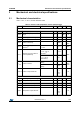
Register description 8.4 LPS25HB WHO_AM_I (0Fh) Device who am I 8.5 7 6 5 4 3 2 1 0 1 0 1 1 1 1 0 1 4 3 2 1 0 AVGT1 AVGT0 AVGP1 AVGP0 RES_CONF (10h) Pressure and temperature resolution 7 6 5 Reserved AVGT[1:0] Temperature internal average configuration. Default: 11 Refer to Table 18 for all the configurations AVGP[1:0] Pressure internal average configuration. Default: 11 Refer to Table 19 for all the configurations Table 18.
LPS25HB 8.6 Register description CTRL_REG1 (20h) Control register 1 7 6 5 4 3 2 1 0 PD ODR2 ODR1 ODR0 DIFF_EN BDU RESET_AZ SIM PD Power-down control. Default value: 0 (0: power-down mode; 1: active mode) ODR [2:0] Output data rate selection. Default value: 000 Refer to Table 20. DIFF_EN Interrupt generation enable. Default value: 0 (0: interrupt generation disabled; 1: interrupt generation enabled) BDU Block data update.
Register description LPS25HB output registers is not updated until both MSB and LSB are read, avoiding the reading of values related to different samples. The RESET_AZ bit is used to reset the AutoZero function. Resetting REF_P_H (0Ah), REF_P_L (09h) and REF_P_XL (08h) sets the pressure reference registers RPDS_H (3Ah) and RPDS_L (39h) to the default value. RESET_AZ is self-cleared. For the AutoZero function please refer to CTRL_REG2 (21h).
LPS25HB Register description the device. These values are factory trimmed and they are different for every device. They allow correct behavior of the device and normally they should not be changed. The boot process takes 2.2 msec. At the end of the boot process, the BOOT bit is set to ‘0’ automatically. FIFO_MEAN_DEC bit is to decimate the output pressure to 1Hz with FIFO Mean mode. When this bit is ‘1’, the output is decimated to 1 Hz as the moving average is being taken at the rate of the ODR.
Register description LPS25HB The device features one set of programmable interrupt sources (INT) that can be configured to trigger different pressure events. Figure 19 shows the block diagram of the interrupt generation block and output pressure data.
LPS25HB 8.10 Register description INTERRUPT_CFG (24h) Interrupt configuration 7 6 5 4 3 Reserved 2 1 0 LIR PL_E PH_E LIR Latch interrupt request to the INT_SOURCE (25h) register. Default value: 0. (0: interrupt request not latched; 1: interrupt request latched) PL_E Enable interrupt generation on differential pressure low event. Default value: 0.
Register description LPS25HB Figure 21. Differential threshold interrupt behavior, LIR = 1 'LIIHUHQWLDO SUHVVXUH K3D /,5 7KV 7KUHVKROG K3D 7LPH VHF 7KV 7KUHVKROG K3D ,$ ,17SLQ 3+ 3/ 7LPH VHF ,17B6285&( UHDG 8.11 INT_SOURCE (25h) Interrupt source 7 6 5 4 3 2 1 0 0 0 0 0 0 IA PL PH IA Interrupt active. (0: no interrupt has been generated; 1: one or more interrupt events have been generated). PL Differential pressure Low.
LPS25HB 8.12 Register description STATUS_REG (27h) Status register 7 6 RES 5 4 P_OR T_OR 3 2 RES 1 0 P_DA T_DA P_OR Pressure data overrun. (0: no overrun has occurred; 1: new data for pressure has overwritten the previous one) T_OR Temperature data overrun. (0: no overrun has occurred; 1: a new data for temperature has overwritten the previous one) P_DA Pressure data available.
Register description 8.14 LPS25HB PRESS_OUT_L (29h) Pressure output value (mid part) 15 14 13 12 11 10 9 8 POUT15 POUT14 POUT13 POUT12 POUT11 POUT10 POUT9 POUT8 POUT[15:8] 8.15 This register contains the mid part of the pressure output value. Refer to PRESS_OUT_XL (28h). PRESS_OUT_H (2Ah) Pressure output value (MSB) 23 22 21 20 19 18 17 16 POUT23 POUT22 POUT21 POUT20 POUT19 POUT18 POUT17 POUT16 POUT[23:16] 8.
LPS25HB 8.17 Register description TEMP_OUT_H (2Ch) Temperature output value (MSB) 15 14 13 12 11 10 9 8 TOUT15 TOUT14 TOUT13 TOUT12 TOUT11 TOUT10 TOUT9 TOUT8 TOUT[15:8] This register contains the high part of the temperature output value. The temperature output value is a 16-bit data that contains the measured temperature. It is composed by TEMP_OUT_H (2Ch) and TEMP_OUT_L (2Bh). The value is expressed as 2’s complement. 8.
Register description LPS25HB Table 23. Running average sample size WTM_POINT[4:0] FIFO Mean mode sample size 00001 2-sample moving average 00011 4-sample moving average 00111 8-sample moving average 01111 16-sample moving average 11111 32-sample moving average Please note that when using the FIFO Mean mode it is not possible to access the FIFO content. 8.
LPS25HB 8.20 Register description THS_P_L (30h) Least significant bits of the threshold value for pressure interrupt generation. 7 6 5 4 3 2 1 0 THS7 THS6 THS5 THS4 THS3 THS2 THS1 THS0 THS[7:0] This register contains the low part of threshold value for pressure interrupt generation. The threshold value for pressure interrupt generation is a 16-bit register composed of THS_P_H (31h) and THS_P_L (30h). The value is expressed as unsigned number: Interrupt threshold(hPA) = (THS_P)/16. 8.
Package mechanical data 9 LPS25HB Package mechanical data In order to meet environmental requirements, ST offers these devices in different grades of ECOPACK® packages, depending on their level of environmental compliance. ECOPACK® specifications, grade definitions and product status are available at: www.st.com. ECOPACK® is an ST trademark. Figure 22. HLGA-10L (2.5 x 2.5 x 0.76 mm typ.) outline and mechanical data 3LQ ,QGLFDWRU 3LQ LQGLFDWRU B Table 24. HLGA-10L (2.5 x 2.
LPS25HB 9.1 Package mechanical data HLGA-10 packing information Figure 23. Carrier tape information for HLGA-10L Figure 24.
Package mechanical data LPS25HB Figure 25. Reel information for carrier tape of HLGA-10L 7 PP PLQ $FFHVV KROH DW VORW ORFDWLRQ % & $ 1 ' )XOO UDGLXV * PHDVXUHG DW KXE 7DSH VORW LQ FRUH IRU WDSH VWDUW PP PLQ ZLGWK Table 25. Reel dimensions for carrier tape of HLGA-10L Reel dimensions (mm) 48/50 A (max) 330 B (min) 1.5 C 13 ±0.25 D (min) 20.2 N (min) 60 G 12.4 +2/-0 T (max) 18.
LPS25HB 10 Revision history Revision history Table 26. Document revision history Date Revision 30-Oct-2014 1 Initial release 2 Updated Table 1: Device summary. Minor update in Figure 2: Pin connections (bottom view), Figure 5: LPS25HB electrical connections (top view), Section 4: FIFO, Section 8.1: REF_P_XL (08h), Section 8.15: PRESS_OUT_H (2Ah) and Figure 12: Interrupt generation block and output pressure data.
LPS25HB IMPORTANT NOTICE – PLEASE READ CAREFULLY STMicroelectronics NV and its subsidiaries (“ST”) reserve the right to make changes, corrections, enhancements, modifications, and improvements to ST products and/or to this document at any time without notice. Purchasers should obtain the latest relevant information on ST products before placing orders. ST products are sold pursuant to ST’s terms and conditions of sale in place at the time of order acknowledgement.