
Data Sheet

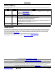

ISL85410
17
FN8375.5
July 24, 2014
Submit Document Feedback
Buck Regulator Output Capacitor Selection
An output capacitor is required to filter the inductor current. The
current mode control loop allows the use of low ESR ceramic
capacitors and thus supports very small circuit implementations
on the PC board. Electrolytic and polymer capacitors may also be
used.
While ceramic capacitors offer excellent overall performance
and reliability, the actual in-circuit capacitance must be
considered. Ceramic capacitors are rated using large
peak-to-peak voltage swings and with no DC bias. In the DC/DC
converter application, these conditions do not reflect reality. As a
result, the actual capacitance may be considerably lower than
the advertised value. Consult the manufacturers data sheet to
determine the actual in-application capacitance. Most
manufacturers publish capacitance vs DC bias so that this effect
can be easily accommodated. The effects of AC voltage are not
frequently published, but an assumption of ~20% further
reduction will generally suffice. The result of these
considerations may mean an effective capacitance 50% lower
than nominal and this value should be used in all design
calculations. Nonetheless, ceramic capacitors are a very good
choice in many applications due to their reliability and extremely
low ESR.
The following equations allow calculation of the required
capacitance to meet a desired ripple voltage level. Additional
capacitance may be used.
For the ceramic capacitors (low ESR):
where I is the inductor’s peak-to-peak ripple current, f
SW
is the
switching frequency and C
OUT
is the output capacitor.
If using electrolytic capacitors then:
Loop Compensation Design
When COMP is not connected to VCC, the COMP pin is active for
external loop compensation. The ISL85410 uses constant
frequency peak current mode control architecture to achieve a
fast loop transient response. An accurate current sensing pilot
device in parallel with the upper MOSFET is used for peak current
control signal and overcurrent protection. The inductor is not
considered as a state variable since its peak current is constant,
and the system becomes a single order system. It is much easier
to design a type II compensator to stabilize the loop than to
implement voltage mode control. Peak current mode control has
an inherent input voltage feed-forward function to achieve good
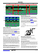
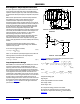
line regulation. Figure 47
shows the small signal model of the
synchronous buck regulator.
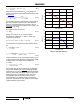
Figure 48
shows the type II compensator and its transfer function
is expressed as shown in Equation 8:
where
,
Compensator design goal:
High DC gain
Choose loop bandwidth f
c
less than 100kHz
Gain margin: >10dB
Phase margin: >40°
The compensator design procedure is as follows:
The loop gain at crossover frequency of f
c
has a unity gain.
Therefore, the compensator resistance R
6
is determined by
Equation 9
.
V
OUTripple
I
8
f
SW
C
OUT
-------------------------------------
=
(EQ. 6)
V
OUTripple
I*ESR=
(EQ. 7)
d
V
in
dI
L
in
in
i
+
1:D
+
L
i
Co
Rc
-Av(S)
d
V
comp
Fm
He(S)
+
T
i
(S)
K
o
v
T
v
(S)
I
L
P
+
1:D
+
Rc
Ro
-Av(S)
R
T
Fm
He(S)
T
K
o
T(S)
^
^
V
^^
^
^
^
^
FIGURE 47. SMALL SIGNAL MODEL OF SYNCHRONOUS BUCK
REGULATOR
R
LP
GAIN (VLOOP (S(fi))
-
+
R
6
V
V
Vo
GM
V
C
7
-
+
C
6
V
REF
V
FB
Vo
V
COMP
FIGURE 48. TYPE II COMPENSATOR
C
3
R
2
R
3
A
v
S
v
ˆ
COMP
v
ˆ
FB
--------------------
GM R
3
C
6
C
7
+R
2
R
3
+
--------------------------------------------------------
1
S
cz1
-------------
+
1
S
cz2
-------------
+
S1
S
cp1
-------------
+
1
S
cp2
-------------
+
---------------------------------------------------------------
==
(EQ. 8)
cz1
1
R
6
C
6
---------------
cz2
1
R
2
C
3
---------------
=
cp1
C
6
C
7
+
R
6
C
6
C
7
-----------------------
cp2
R
2
R
3
+
C
3
R
2
R
3
-----------------------
==,=