
Data Sheet

GP2Y0D815Z0F
3
Sheet No.: OP14005EN
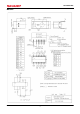
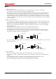
Signal
processing circuit
Measuring distance IC
R1 (LED current adjustment resistance=4.3Ω (LED Pulse current TYP 70mA)
C1・C2=0.1μF
■Schematic
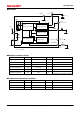
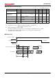
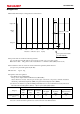
■Absolute maximum ratings
Parameter
Symbol
Ratings
Unit
Remark
Supply voltage
Vcc
-0.3 to +7
V
-
Output terminal voltage
Vo
-0.3 to Vcc+0.3
V
-
Input terminal voltage
Vin
-0.3 to Vcc+0.3
V
-
Operating temperature
Topr
-10 to +60
°C
-
Storage temperature
Tstg
-20 to +70
°C
-
Soldering temperature
Tsol
260
°C
5s or less/time up 2 times
t=1.0mm One side borad mounting
■Recommended operating conditions
Parameter
Symbol
Rating
Unit
Remark
Supply voltage
Vcc
2.7 to 6.2
V
-
High level input voltage
VinH
MIN Vcc-0.2
V
CMOS level signal. Operating
Low level input voltage
VinL
MAX 0.2
V
CMOS level signal. Standby state
GND
Vcc
LED
PD
Vo
REG
LED_FB
C1
R1
Vcc
Vin
LED
Anode
Cathode
Voltage regulator
Oscillation circuit
Output circuit
LED drive circuit
C2