
Data Sheet


DMOS Microstepping Driver with Translator
and Overcurrent Protection
A4988
18
Allegro MicroSystems, Inc.
115 Northeast Cutoff
Worcester, Massachusetts 01615-0036 U.S.A.
1.508.853.5000; www.allegromicro.com
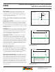
Pin-out Diagram
Terminal List Table
Name Number Description
CP1 4 Charge pump capacitor terminal
CP2 5 Charge pump capacitor terminal
VCP 6 Reservoir capacitor terminal
VREG 8 Regulator decoupling terminal
MS1 9 Logic input
MS2 10 Logic input
MS3 11 Logic input
¯
R
¯
¯
E
¯
¯
S
¯
¯
E
¯
¯
T
¯
12 Logic input
ROSC 13 Timing set
¯
S
¯
¯
L
¯
¯
E
¯
¯
E
¯
¯
P
¯
14 Logic input
VDD 15 Logic supply
STEP 16 Logic input
REF 17 G
m
reference voltage input
GND 3, 18 Ground*
DIR 19 Logic input
OUT1B 21 DMOS Full Bridge 1 Output B
VBB1 22 Load supply
SENSE1 23 Sense resistor terminal for Bridge 1
OUT1A 24 DMOS Full Bridge 1 Output A
OUT2A 26 DMOS Full Bridge 2 Output A
SENSE2 27 Sense resistor terminal for Bridge 2
VBB2 28 Load supply
OUT2B 1 DMOS Full Bridge 2 Output B
¯
E
¯
¯
N
¯
¯
A
¯
¯
B
¯
¯
L
¯
¯
E
¯
2 Logic input
NC 7, 20, 25 No connection
PAD – Exposed pad for enhanced thermal dissipation*
*The GND pins must be tied together externally by connecting to the PAD ground plane
under the device.
PAD
21
20
19
18
17
16
15
1
2
3
4
5
6
7
8
9
10
11
12
13
14
28
27
26
25
24
23
22
VBB2
SENSE2
OUT2A
NC
OUT1A
SENSE1
VBB1
VREG
MS1
MS2
MS3
RESET
ROSC
SLEEP
OUT1B
NC
DIR
GND
REF
STEP
VDD
OUT2B
ENABLE
GND
CP1
CP2
VCP
NC