
Data Sheet

New Product
TSSP77038
www.vishay.com
Vishay Semiconductors
Rev. 1.0, 09-Mar-12
2
Document Number: 82470
THIS DOCUMENT IS SUBJECT TO CHANGE WITHOUT NOTICE. THE PRODUCTS DESCRIBED HEREIN AND THIS DOCUMENT
ARE SUBJECT TO SPECIFIC DISCLAIMERS, SET FORTH AT www.vishay.com/doc?91000
Note
• Stresses beyond those listed under “Absolute Maximum Ratings” may cause permanent damage to the device. This is a stress rating only
and functional operation of the device at these or any other conditions beyond those indicated in the operational sections of this specification
is not implied. Exposure to absolute maximum rating conditions for extended periods may affect the device reliability.
TYPICAL CHARACTERISTICS (T
amb
= 25 °C, unless otherwise specified)
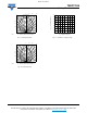
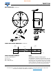
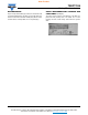
Fig. 1 - Output Active Low Fig. 2 - Pulse Length and Sensitivity in Dark Ambient
ABSOLUTE MAXIMUM RATINGS
PARAMETER TEST CONDITION SYMBOL VALUE UNIT
Supply voltage V
S
- 0.3 to + 6 V
Supply current I
S
5mA
Output voltage V
O
- 0.3 to (V
S
+ 0.3) V
Output current I
O
5mA
Junction temperature T
j
100 °C
Storage temperature range T
stg
- 25 to + 85 °C
Operating temperature range T
amb
- 25 to + 85 °C
Power consumption T
amb
≤ 85 °C P
tot
10 mW
ELECTRICAL AND OPTICAL CHARACTERISTICS (T
amb
= 25 °C, unless otherwise specified)
PARAMETER TEST CONDITION SYMBOL MIN. TYP. MAX. UNIT
Supply voltage V
S
2.5 5.5 V
Supply current
V
S
= 5 V, E
v
= 0 I
SD
0.55 0.7 0.9 mA
E
v
= 40 klx, sunlight I
SH
0.8 mA
Transmission distance
E
v
= 0,
IR diode TSAL6200,
I
F
= 250 mA,
test signal see fig. 1
d40m
Output voltage low
I
OSL
= 0.5 mA, E
e
= 0.7 mW/m
2
,
test signal see fig. 1
V
OSL
100 mV
Minimum irradiance
Pulse width tolerance:
t
pi
- 5/f
o
< t
po
< t
pi
+ 6/f
o,
test signal see fig. 1
E
e min.
0.2 0.4 mW/m
2
Maximum irradiance
t
pi
- 5/f
o
< t
po
< t
pi
+ 6/f
o
,
test signal see fig. 1
E
e max.
50 W/m
2
Directivity
Angle of half transmission
distance
ϕ
1/2
± 50 deg
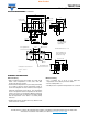
E
e
T
t
pi
*
t
* t
pi
10/f
0
is recommended for optimal function
V
O
V
OH
V
OL
t
16110
Optical Test Signal
(IR diode TSAL6200, I
F
= 0.4 A, 30 pulses, f = f
0
, t = 10 ms)
Output Signal
t
d
1)
t
po
2)
1)
7/f
0
< t
d
< 15/f
0
2)
t
pi
- 5/f
0
< t
po
< t
pi
+ 6/f
0
0
0.1
0.2
0.3
0.4
0.5
0.6
0.7
0.8
0.9
1.0
1.1
1.2
1.3
1.4
1.5
0.1 10 1000 100 000
t
po
- Output Pulse Width (ms)
E
e
- Irradiance (mW/m
2
)
Output pulse width
Input burst length
λ = 950 nm,
optical test signal, Fig. 1