
Data Sheet

FinalDatasheet 6 Rev.1.0, 2008-09-18
TLE4946-2K
Functional Description
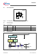
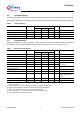
2.2 Pin Configuration
Center of
Sensitive Area
1
± 0.15
1.5
± 0.15
0.8
2
3
SC59
Figure 1 Pin Configuration and sensitive area (Top View, Figure not to Scale)
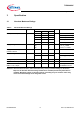
2.3 Pin Description
Table 1 Pin Description
Pin or Ball
No.
Name Pin
Type
Function Comments
1 Vs I Supply voltage
2 Q O Output
3
GND I Ground
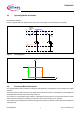
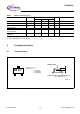
2.4 Block Diagram
Ref
Chopped
Hall Probe
V
S
Q
GND
Amplifier
Low
Pass
Filter
Comparator
with
Hysteresis
Voltage Regulator
reverse polarity protected
Oscillator
and
Sequencer
Bias and
Compensation
Circuits
Figure 2 TLE4946-2K Block Diagram