September 2008 TLE4946-2K High Precision Hall Effect Latch TLE4946-2K Final Datasheet R e v. 1 .
Edition 2008-09-18 Published by Infineon Technologies AG 81726 München, Germany © 2007 Infineon Technologies AG All Rights Reserved. Legal Disclaimer The information given in this document shall in no event be regarded as a guarantee of conditions or characteristics.
TLE4946-2K TLE4946-2K High Precision Hall Effect Latch Revision History: 2008-09-18, Rev.1.0 Previous Version: Page Subjects (major changes since last revision) We Listen to Your Comments Any information within this document that you feel is wrong, unclear or missing at all? Your feedback will help us to continuously improve the quality of this document. Please send your proposal (including a reference to this document) to: sensors@infineon.com FinalDatasheet 3 Rev.1.
TLE4946-2K 1 1.1 1.2 1.3 Product Description 5 Overview 5 Features 5 Target Applications 5 2 2.1 2.2 2.3 2.4 2.5 2.6 Functional Description 5 General 5 Pin Configuration 6 Pin Description 6 Block Diagram 6 Operating Modes and States 7 Functional Block Description 7 3 3.1 3.2 3.3 Specification 8 Absolute Maximum Ratings 8 Operating Range 9 Characteristics 9 4 4.1 Package Information 10 Package Outline 10 FinalDatasheet 4 Rev.1.
High Precision Hall Effekt Latch 1 Product Description 1.1 Overview TLE4946-2K The TLE4946-2K is a high precision Hall effect latch with highly accurate switching thresholds for operating temperatures up to 150°C. 1.2 • • • • • • • • • • • Features 2.
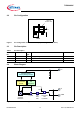
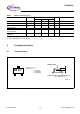
TLE4946-2K Functional Description 2.2 Pin Configuration Center of Sensitive Area 3 0.8 1 1.5 ± 0.15 2 ± 0.15 SC59 Figure 1 Pin Configuration and sensitive area (Top View, Figure not to Scale) 2.3 Pin Description Table 1 Pin Description Pin or Ball No. Name Pin Type Function 1 Vs I Supply voltage 2 Q O Output 3 GND I Ground 2.
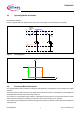
TLE4946-2K Functional Description 2.5 Operating Modes and States Field Direction Definition: Positive magnetic fields are related with the south pole of the magnet to the branded side of package. B OP Applied Magnetic Field B RP td td tf VQ tr 90% 10% Figure 3 Timing diagram VQ B B rp 0 Figure 4 Output Signal 2.6 Functional Block Description Bop The chopped Hall IC switch comprises a Hall probe, bias generator, compensation circuits, oscillator and output transistor.
TLE4946-2K Specification 3 Specification 3.1 Absolute Maximum Ratings Table 2 Absolute Maximum Ratings Parameter Symbol Values Unit Note/Test Condition Min. Typ. Max. -40 – 150 – – 155 for 2000 h (not additive) – – 165 for 1000 h (not additive) – – 175 for 168 h (not additive) – – 195 for 3 x 1 h (additive) VDD -18 -18 -18 – – – 18 24 26 V Supply current through protection device IS – 50 – + 50 mA Output voltage VQ -0.7 – 18 V -0.
TLE4946-2K Specification 3.2 Operating Range The following operating conditions must not be exceeded in order to ensure correct operation of the TLE4946-2K. All parameters specified in the following sections refer to these operating conditions unless otherwise mentioned. Table 3 Operating Range Parameter Symbol Min. Typ. Max. Supply voltage VS 2.7 – 18 V Output voltage VQ – 0.7 – 18 V Junction temperature Tj – 40 – 150 °C Output current IQ 0 – 20 mA 3.
TLE4946-2K Package Information Table 5 Magnetic Characteristics Parameter Symbol Values Unit Min. Typ. Max. Operate point BOP 0.5 2.0 3.5 mT Release point BRP BHYS -3.5 -2.0 -0.5 mT 1.0 4 6.0 mT Magnetic Offset BOFF -1.5 0 1.5 mT Temperature compensation of magn.
TLE4946-2K Package Information 1.1 ±0.1 3 ±0.1 0.1 2.8 +0.2 -0.1 3 1 +0.1 1.6 +0.15 -0.3 0.1 0.2 M 0.45 ±0.15 3x0.4 +0.05 -0.1 0.15 MAX. 2 +0.1 0.15 -0. 05 0.1 M 0.95 0.95 (0.55) 0˚...8˚ MAX. GPS09473 Figure 6 Package outline 0.8 1.4 min 0.9 1.6 1.3 0.9 1.4 min 0.8 1.2 0.8 1.2 0.8 Reflow Soldering Figure 7 Wave Soldering Footprint SC59 (SOT23 compatible) FinalDatasheet 11 Rev.1.
www.infineon.
Mouser Electronics Authorized Distributor Click to View Pricing, Inventory, Delivery & Lifecycle Information: Infineon: TLE4946-2K