
User Manual

01-Jan-2008 Rev. B
Page 5 of 7
http://www.SeCoSGmbH.com/ Any changing of specification will not be informed individual
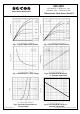
N-Channel
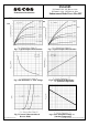
Fig 10. Effective Transient Thermal ImpedanceFig 9. Maximum Safe Operating Area
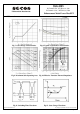
Fig 8. Typical Capacitance CharacteristicsFig 7. Gate Charge Characteristics
Fig 11. Switching Time Waveform
Fig 12. Gate Charge Waveform
Elektronische Bauelemente
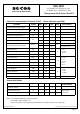
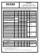
SSG4505
N Channel 10A, 30V,RDS(ON) 14m
Enhancement Mode Power Mos.FET
P Channel -8.4A, -30V,RDS(ON) 20m
Ω
Ω