
User Manual
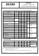
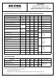

Electrical Characteristics P-Channel( Tj=25 C Unless otherwise specified)
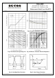
Total Gate Charge
RDS(ON)
Parameter Symbol Max.
Typ.
Test Condition
Min.
Unit
Drain-Source Breakdown Voltage
Breakdown Voltage Temp. Coefficient
Gate Threshold Voltage
Gate-Source Leakage Current
Drain-Source Leakage Current (Tj=25 )
Static Drain-Source On-Resistance
Drain-Source Leakage Current (Tj=70
)
Gate-Source Charge
Gate-Drain ("Miller") Charge
Turn-on Delay Time
Rise Time
Turn-off Delay Time
Fall Time
Input Capacitance
Output Capacitance
Reverse Transfer Capacitance
BVDSS
BVDS/ Tj
VGS(th)
IGSS
IDSS
Crss
Qg
Qgs
Qgd
Td(ON)
Td
(Off)
Tr
Ciss
Coss
T
f
-30
-0.02
-1.0
100
-1
-25
20
30
27
4
18
16
11
40
25
1580
540
450
±
V
V/
V
nA
uA
uA
m
nC
nS
pF
Ω
VGS=0V
VDS=-25V
f=1.0MHz
VDS=-15V
ID=-1A
VGS=-10V
RG=3.3
RD=15
Ω
Ω
ID=-8A
VDS=-24V
VGS=-4.5V
VGS=-10V, ID=-8A
VGS=-4.5V, ID=-4A
VGS=0V, ID=-250uA
VGS= 20V
±
VDS=-30V,VGS=0
VDS=-24V,VGS=0
VDS=VGS, ID=-250uA
Reference to 25 , ID=-1mA
_
_
_
_
_
_
_
_
_
_
_
_
_
_
_
_
_
_
_
_
_
_
_
_
_
_
_
_
_
_
_
_
_
2
Forward Transconductance
Gfs
S
14
VDS=-10V, ID=-8A
_
_
_
C
o
C
o
C
o
C
o
2
2
45
2530
-3.0
o
Source-Drain Diode
Parameter Symbol Max.
Typ.
Test Condition
Min. Unit
Forward On Voltage
Reverse Recovery Time
V
SD
Trr
__
_
_
IS=-1.7A, VGS=0V
IS=-8A,VGS=0V
dl/dt=100A/us
V
nS
-1.2
40
2
Reverse Recovery Charge
Qrr
_
_
nC
32
http://www.SeCoSGmbH.com/ Any changing of specification will not be informed individual
01-Jan-2008 Rev. B
Page 3 of 7
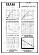
Notes: 1.Pulse width limited by Max. junction temperature.
2.Pulse width 300us, dutycycle 2%.
≦
≦
3.Surface mounted on 1 inch2 copper pad of FR4 board;135 when mounted on min. copper pad.
°C/W
Elektronische Bauelemente
SSG4505
N Channel 10A, 30V,RDS(ON) 14m
Enhancement Mode Power Mos.FET
P Channel -8.4A, -30V,RDS(ON) 20m
Ω
Ω