
Datasheet


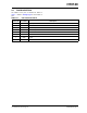


Table Of Contents
- 1.0 Electrical Characteristics
- 2.0 Pin Description
- 3.0 Functional Description
- 4.0 Packaging Information
- 4.1 Package Marking Information
- Information contained in this publication regarding device applications and the like is provided only for your convenience and may be superseded by updates. It is your responsibility to ensure that your application meets with your specifications. MIC...
- Trademarks
- The Microchip name and logo, the Microchip logo, AnyRate, dsPIC, FlashFlex, flexPWR, Heldo, JukeBlox, KeeLoq, KeeLoq logo, Kleer, LANCheck, LINK MD, MediaLB, MOST, MOST logo, MPLAB, OptoLyzer, PIC, PICSTART, PIC32 logo, RightTouch, SpyNIC, SST, SST L...
- ClockWorks, The Embedded Control Solutions Company, ETHERSYNCH, Hyper Speed Control, HyperLight Load, IntelliMOS, mTouch, Precision Edge, and QUIET-WIRE are registered trademarks of Microchip Technology Incorporated in the U.S.A.
- Analog-for-the-Digital Age, Any Capacitor, AnyIn, AnyOut, BodyCom, chipKIT, chipKIT logo, CodeGuard, dsPICDEM, dsPICDEM.net, Dynamic Average Matching, DAM, ECAN, EtherGREEN, In-Circuit Serial Programming, ICSP, Inter-Chip Connectivity, JitterBlocker,...
- SQTP is a service mark of Microchip Technology Incorporated in the U.S.A.
- Silicon Storage Technology is a registered trademark of Microchip Technology Inc. in other countries.
- GestIC is a registered trademarks of Microchip Technology Germany II GmbH & Co. KG, a subsidiary of Microchip Technology Inc., in other countries.
- All other trademarks mentioned herein are property of their respective companies.
- © 2016, Microchip Technology Incorporated, Printed in the U.S.A., All Rights Reserved.
- ISBN: 978-1-5224-1004-1
- AMERICAS
- ASIA/PACIFIC
- ASIA/PACIFIC
- EUROPE
- 4.1 Package Marking Information

2016 Microchip Technology Inc. DS20005628A-page 3
HT0740
1.0 ELECTRICAL CHARACTERISTICS
Absolute Maximum Ratings†
Input to Output Isolation Voltage, V
ISO
................................................................................................................. ±400V
Logic Input Voltage, V
IN
..............................................................................................................................–0.5V to +7V
Operating Ambient Temperature, T
A
......................................................................................................–40°C to +85°C
Storage Temperature, T
S
......................................................................................................................–55°C to +150°C
† Notic
e: Stresses above those listed under “Absolute Maximum Ratings” may cause permanent damage to the
device. This is a stress rating only, and functional operation of the device at those or any other conditions above those
indicated in the operational sections of this specification is not intended. Exposure to maximum rating conditions for
extended periods may affect device reliability.
RECOMMENDED OPERATING CONDITIONS
Parameter Sym. Min. Typ. Max. Unit Conditions
Logic Input High Voltage V
IH
3.15 — 5.5 V
Logic Input Low Voltage V
IL
0 — 0.5 V
Operating Ambient
T
emperature
T
A
–40 — +85 °C
DC ELECTRICAL CHARACTERISTICS
Electrical Specifications: T
A
= 25°C unless otherwise indicated.
Parameter Sym. Min. Typ. Max. Unit Conditions
Logic High Input Current I
H
— — 500 µA V
IN
= 5V
Logic Low Input Current
(Qu
iescent)
I
L
— — 10 µA V
IN
= 0.5V
Output Voltage Across Output
T
erminals
V
OUT
4.5 — — V V
IN
= 3.15V, no load
8.5 — — V V
IN
= 4.5V, no load
Input Voltage for Zero Output V
IN
— — 0.8 V No load
Input to Output Isolation
Voltage
V
ISO
±400 — — V
AC ELECTRICAL CHARACTERISTICS
Electrical Specifications: T
A
= 25°C unless otherwise indicated.
Parameter Sym. Min. Typ. Max. Unit Conditions
Turn-on Delay Time t
d(ON)
— — 50 µs
See Figure 3-1 and Figure 3-2.
C
L
= 600 pF, T
A
= 25 °C
Rise Time t
r
— — 650 µs
Turn-off Delay Time t
d(OFF)
— — 150 µs
Fall Time t
f
— — 3 ms