Pico Computing Pico E-15 Hardware Technical Reference Release: 1.01 For Hardware Revision: D www.picocomputing.com (206) 283-2178 Pico Computing 150 Nickerson Street.
Contents: Product Overview Quick Reference Datasheet Standard Part Numbers System Architecture Electrical Specification 3 4 5 6 7 Features Field Programmable Gate Array PowerPC™ Processor CPLD TurboLoader Flash Memory DDR2 SDRAM Memory Temperature Sensor 8 9 10 11 12 14 I/O Interfaces Sleep Controller Tri-Mode Ethernet Interface Digital Peripheral Interface High Speed Analog to Digital Converters High Speed Digital to Analog Converters Video Digitizer CardBus / Digital Bus Interface JTAG Debug Interf
Product Overview: The Pico family of products are revolutionary FPGA based embedded acceleration platforms. With performance that often exceeds modern microcomputers, a shockingly small form factor, and nominal power consumption that is less than one watt, the Pico family of products take computing to a whole new level. The Pico E-15 is based on the high-performance Virtex-4 FPGA chip.
Pico E-15 Quick Reference Datasheet FEATURES ♦ ♦ ♦ ♦ ♦ ♦ ♦ ♦ ♦ ♦ MECHANICAL High-performance Virtex-4 FX-20, 40 or 60 256MB RAM 64MB Flash ROM Dual 12-Bit 125 MSPS A/D converters Dual 14-Bit 210 MSPS D/A converters Integrated composite video capture CardBus (PCI) Interface Open source Standalone operation Reconfigurable, high-speed digital bus Temperature Range: 0°C to +70°C PC Card Type II Form-Factor Stainless steel case POWER Sleep: 0.001W Nominal: 1.2W Absolute Maximum: 7.0W Supply Voltage: 3.
Standard Part Numbers Standard Part Number FX-20 FX-40 FX-60 E15FX20-256/64/JEGSAADDV10C E15FX40-256/64/JEGSAADDV10C E15FX60-256/64/JEGSAADDV10C A Military version is available which includes: BGA underfill Conformal coating Extended temperature range The Military version is available by special order only, and is subject to minimum quantity requirements. Pico E-15 Hardware Reference www.picocomputing.com (206) 283-2178 Pico Computing 150 Nickerson Street.
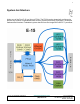
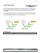
System Architecture At the core of the Pico E-15 is a Virtex-4 FPGA. The FPGA can be dynamically configured to perform any number of specialized tasks such as: protocol processing, encryption, or complex mathematical functions. Embedded systems benefit from the integrated PowerPC™ processor. Pico E-15 Hardware Reference www.picocomputing.com (206) 283-2178 Pico Computing 150 Nickerson Street.
Pico E-15 Electrical Specification Minimum Nominal Maximum DC Input Voltage Power Consumption DC Input Current 3.25V 0.001W 0.0003A 3.3V 1.2W 0.36A 3.35V 7.0W 2.1A Recommended Temperature Range FPGA Over Temperature Shutdown Maximum Storage Temperature Range Relative Humidity (Non-Condensing) 0°C 10°C 70-80°C 27°C 70°C -50°C 0% 90°C 95% Overpower Considerations: The Pico E-15 FX60 is designed desktop computers, and is not recommended for use in laptops.
Field Programmable Gate Array The core of the Pico E-15 is a high performance Virtex-4 FPGA. Included in the FPGA are the FPGA Fabric, an optional PowerPC ™ processor, ultra high-speed DSP slices and RAM. FPGA Fabric: The “Fabric” of an FPGA comprises an array of logic elements that can be connected in virtually unlimited patterns.
PowerPC™ Processor PPC405x3 Processor Introduction: FPGAs are renowned for their ability to process parallel logic, but they typically have a hard time emulating a high performance processor. To get the best of both worlds the Virtex-4™ features an embedded Power PC Processor. Since the processor shares the same die as the FPGA it seamlessly interfaces with the FPGA fabric. A new feature of the Virtex-4 FPGA is the addition of an auxiliary processor interface.
CPLD TurboLoader A CPLD (Complex Programmable Logic Device) is a smaller version of an FPGA (described above) with permanent Flash storage built in. The Pico E-15 contains one CPLD that loads and reconfigures the FPGA. The Pico firmware guide describes how to access the CPLD TurboLoader. The Flash ROM’s address bus can be controlled by either the TurboLoader or the FPGA (but not both). During power-up or reboot, the TurboLoader is in control of the Flash ROM Address bus.
Flash Memory The Pico E-15 comes equipped with at least 64MB of Flash ROM. The Flash ROM is divided into 512 sectors that can be erased independently. Most of the space on the ROM is reserved for the user. The Flash ROM’s address bus can be controlled by either the TurboLoader or the FPGA (but not both). During power-up or reboot, the TurboLoader is in control of the Flash ROM Address bus. At all other times the FPGA is in control of the address bus.
DDR2 SDRAM Memory The Pico E-15 comes equipped with 256MB of DDR2 SDRAM memory. There are two 1024Mb chips, each with a separate 16 bit data path to the host to form one 32 bit bank. From 0°C to +85°C, the ram can run at up to 333 MHz. For operation at temperatures below 0°C, special firmware with throttled ram timings is required. Please note that the RAM will not function below 125 MHz. Virtex-4 FPGA RAM MSBs RAM LSBs Pico E-15 Hardware Reference www.picocomputing.
RAM Timing and Parameter Information Parameter Value EDK Value 133 MHz EDK Value 333 MHz Registered Clock Pairs Memory Banks IDELAY Controllers Differential DQs Open Row Management On Die Termination ECC Support TMRD TWR TWTR TRAS TRC TRFC TRCD TRRD TRP TREFI TFAW CAS Latency Data Width Address Width Column Width Bank Address Width Clock Period* No 1 1 2 Yes No Disabled No 2 Clocks 15 nS 7.5 nS 45 nS 60 nS 127.5 nS 15 nS 10 nS 15 nS 7.8 uS 37.
Temperature Sensor The Pico E-15 contains one temperature sensor that directly senses the die temperature of the Virex-4 FPGA. The digital interface of the remote temperature sensing chip is connected to the Cypress PSoC. If an overtemperature condition occurs, the PSoC will shutdown the FPGA until the temperature has dropped sufficiently below the shutdown threshold. The setpoints of the temperature shutdown circuit can be reprogrammed via the PSoC debug cable.
Sleep Controller The Pico E-15 contains one Cypress PSoC which is used to generate a clock for the bootloader and control the power state. The E-15 can be placed in a state where it draws almost no power, then wakes up automatically after a set amount of time. The sleep controller can be activated by the FPGA, or the external peripheral interface connector. The protocol for entering sleep state is simple.
Tri-Mode Ethernet Interface The Pico E-15 features the Marvell Alaska series 88E1111 tri-mode Ethernet transceiver. Combined with the on-FPGA MAC (Middle access controller) a complete Ethernet solution is offered. Communication between the MAC and PHY takes place over an industry standard MII/GMII interface. The Ethernet transceiver features 10/100/1000 full/half duplex operation. It will automatically configure the physical interface on the fly for crossover or straight through operation.
Digital Peripheral Interface The Pico E-15 features 2 GPIO lines which are used for external peripheral support. The GPIO lines are always enabled. All GPIO signals have user selectable pull-up, pull-down, keeper or HI-Z termination. Drive strength is also user selectable between 2 and 24mA. All GPIOs can be configured for input, output and bi-directional mode. GPIO 1 has a 50 ohm resistor in series with the output to allow connectivity with low voltage devices which may clamp a 3.3V signal.
High Speed Analog to Digital Converters The Pico E-15 features 2 high speed analog to digital converters. The converters are optimized for high-frequency, high-performance, low-power, low-noise operation. The converters have integrated DC blocking capacitors, and thus, cannot be used on very low frequency signals. The ADC should be driven by a source with an impedance of 50 ohms. To ensure accuracy at high speeds, the low-jitter 125 MHz reference clock must be used.
Electrical Specifications Minimum Nominal Maximum Differential AC Input Voltage Termination Resistance Input Frequency Range Bandwidth 0 Vpp 45 (VHF) 1 KHz* 1 Vpp 50 (AC) 1-50 MHz 125 MHz 1.8 Vpp 115(DC) 125 MHz 225 MHz Dielectric Surge Withstand Voltage Withstand Voltage -14 VDC -4 VDC 0 VDC 0 VDC 14 VDC 4 VDC 125 MHz 125 MHz 12 Bits 0.007V Clock Frequency Resolution Sensativity 0.087V 0.013V *Lower frequencies are possible with degraded performance.
ADC Low Frequency Input Impedance ADC High Frequency Input Impedance* *Low pass filter range is customizable via special order Pico E-15 Hardware Reference www.picocomputing.com (206) 283-2178 Pico Computing 150 Nickerson Street.
High Speed Digital to Analog Converters The Pico E-15 features 2 high speed analog to digital converters. The converters are optimized for high-frequency, high-performance, low-power, low-noise operation. The converters have integrated DC blocking capacitors, and can not be used on low frequency signals. The DAC should be terminated into a 50 ohm load. To ensure accuracy at high speeds, the low-jitter 125 MHz reference clock must be used. The DAC supports a clock frequency of up to 210 MHz.
DAC Low Frequency Maximum Amplitude (50 Ohm Load) DAC High Frequency Maximum Amplitude (50 Ohm Load) Pico E-15 Hardware Reference www.picocomputing.com (206) 283-2178 Pico Computing 150 Nickerson Street.
Video Digitizer The Pico E-15 contains one ultra low-power video digitizer. The video digitizer accepts both SVIDEO and Composite video inputs and can decode NTSC, PAL and SECAM video standards. When using composite video, the video digitzer can switch from between two channels. The TVP5150 has an integrated I2C control interface.
CardBus / Digital Bus Interface The Pico E-15 can run as a standalone product or be connected to a host using the CardBus connector. By default, the Pico E-15 ships with firmware that is ready for use as a CardBus device. The CardBus interface is a subset of PCI. The data path is 32 bits wide and is synchronous. The wiring of the CardBus interface supports both completion and mastering of the bus.
JTAG Debug Interface The Pico E-15 is equipped with a JTAG diagnostic port which allows real-time debugging of hardware, firmware and software. Some JTAG programs require the length of the instruction register (IR). The IR length is listed below for all devices in the JTAG chain. The FPGA IR length changes depending on how many PowerPCs are internally connected to the JTAG chain in the FPGA.
PSoC Debug Interface The Pico E-15 has a low power PSoC microcontroller (also known as the sleep controller) which controls the power to the rest of the board. The PSoC also generates a 24 MHz clock for the TurboLoader. The PSoC features an in-circuit programming interface, although it is unlinkey that a user will ever need to debug or modify the PSoC firmware.
Appendix A – Peripheral I/O Connector Information Connector Information Description Mating Connector Brand Hirose Part Number NX-32TA-CV1(50) *Connectors are always in stock at Pico Computing Peripheral I/O Connector Pinout 1 2 3 4 5 6 7 8 9 10 11 12 13 14 15 16 17 18 19 20 21 22 23 24 25 26 27 28 29 30 31 32 VIDEO_GND VIDEO_IN_C VIDEO_IN_Y TMS TCK TDI TDO ANALOG_IN_1+ ANALOG_IN_1ETHER_OUT_DAETHER_OUT_DA+ ETHER_OUT_DDETHER_OUT_DD+ ETHER_OUT_DCETHER_OUT_DC+ ETHER_OUT_DBETHER_OUT_DB+ POWERCTL_R ANALO
Peripheral Connector Drawing Figure 5 Pico E-15 Hardware Reference www.picocomputing.com (206) 283-2178 Pico Computing 150 Nickerson Street.
Appendix B – CardBus Connector Information Connector Information Description CardBus Socket Brand FCI Part Number 71299-050CALF The CardBus Socket is typically in stock at Mouser Electronics. (http://www.mouser.com) The function and direction of the pins on the CardBus interface can be easily changed to suit the needs of a custom interface. Series termination on the E-15 is zero ohms, but a larger value can be used if it is required for your application. Pico E-15 Hardware Reference www.
CardBus Interface Schematic Pico E-15 Hardware Reference www.picocomputing.com (206) 283-2178 Pico Computing 150 Nickerson Street.
CardBus Connector Pinout 1 2 3 4 5 6 7 8 9 10 11 12 13 14 15 16 17 18 19 20 21 22 23 24 25 26 27 28 29 30 31 32 33 34 35 36 37 38 39 40 41 42 43 44 45 46 47 48 GND PCI_CAD0 PCI_CAD1 PCI_CAD3 PCI_CAD5 PCI_CAD7 P\C\I\_\C\C\B\E\0\ PCI_CAD9 PCI_CAD11 PCI_CAD12 PCI_CAD14 P\C\I\_\C\C\B\E\1\ PCI_CPAR P\C\I\_\C\P\E\R\R\ P\C\I\_\C\G\N\T\ P\C\I\_\C\I\N\T\ 3.
49 50 51 52 53 54 55 56 58 59 60 61 62 63 64 65 66 67 68 P\C\I\_\C\S\T\O\P\ P\C\I\_C\D\E\V\S\E\L\ 3.3V VPP P\C\I\_\C\T\R\D\Y\ P\C\I\_\C\F\R\A\M\E\ PCI_CAD17 PCI_CAD19 P\C\I\_\C\R\S\T\ P\C\I\_\C\S\E\R\R\ P\C\I\_\C\R\E\Q\ P\C\I\_\C\C\B\E\3\ PCI_CAUDIO PCI_CSTSCHG PCI_CAD28 PCI_CAD30 PCI_CAD31 GND GND Pico E-15 Hardware Reference Transfer Halt Device Select 3.
Appendix C – FPGA Pinout FPGA Pinout Net ADC_1_CLK_IN+ ADC_1_CLK_INADC_1_CLK_RTURN ADC_1_D0 ADC_1_D1 ADC_1_D2 ADC_1_D3 ADC_1_D4 ADC_1_D5 ADC_1_D6 ADC_1_D7 ADC_1_D8 ADC_1_D9 ADC_1_D10 ADC_1_D11 ADC_1_OVERLOAD ADC_1_POWER ADC_2_CLK_IN+ ADC_2_CLK_INADC_2_CLK_RTURN ADC_2_D0 ADC_2_D1 ADC_2_D2 ADC_2_D3 ADC_2_D4 ADC_2_D5 ADC_2_D6 ADC_2_D7 ADC_2_D8 ADC_2_D9 ADC_2_D10 ADC_2_D11 ADC_2_OVERLOAD ADC_2_POWER C\B\L\O\C\K\ C\C\B\E\0\ C\C\B\E\1\ C\C\B\E\2\ C\C\B\E\3\ C\D\E\V\S\E\L\ C\F\R\A\M\E\ C\G\N\T\ Pin K8 K7 D6 G
C\I\N\T\ C\I\R\D\Y\ C\P\E\R\R\ C\R\E\Q\ C\R\S\T\ C\S\E\R\R\ C\S\T\O\P\ C\T\R\D\Y\ CAD0 CAD1 CAD2 CAD3 CAD4 CAD5 CAD6 CAD7 CAD8 CAD9 CAD10 CAD11 CAD12 CAD13 CAD14 CAD15 CAD16 CAD17 CAD18 CAD19 CAD20 CAD21 CAD22 CAD23 CAD24 CAD25 CAD26 CAD27 CAD28 CAD29 CAD30 CAD31 CAUDIO CCLK CCLKRUN CPAR CSTSCHG DAC_1_CLK_IN+ DAC_1_CLK_INDAC_1_D0 DAC_1_D1 DAC_1_D2 F4 D4 H3 A10 A8 A9 F3 D3 AD15 AE15 AF15 AF14 AD14 AC14 AA13 AB12 AC13 AD13 AC12 AA12 AB14 AA14 M6 M5 K3 C4 C7 B6 A7 B7 B9 B10 B11 A12 B12 A13 C8 C13 E10 D10
DAC_1_D3 DAC_1_D4 DAC_1_D5 DAC_1_D6 DAC_1_D7 DAC_1_D8 DAC_1_D9 DAC_1_D10 DAC_1_D11 DAC_1_D12 DAC_1_D13 DAC_1_POWER DAC_2_CLK_IN+ DAC_2_CLK_INDAC_2_D0 DAC_2_D1 DAC_2_D2 DAC_2_D3 DAC_2_D4 DAC_2_D5 DAC_2_D6 DAC_2_D7 DAC_2_D8 DAC_2_D9 DAC_2_D10 DAC_2_D11 DAC_2_D12 DAC_2_D13 DAC_2_POWER ETHER_CLK_TERM ETHER_CLK_TERM ETHER_COL ETHER_CRS ETHER_GTX_TERM ETHER_IRQ ETHER_MDC ETHER_MDIO ETHER_RESET ETHER_RX0 ETHER_RX1 ETHER_RX2 ETHER_RX3 ETHER_RX4 ETHER_RX5 ETHER_RX6 ETHER_RX7 ETHER_RX_CLK ETHER_RX_DV ETHER_RX_ER
ETHER_TX1 ETHER_TX2 ETHER_TX3 ETHER_TX4 ETHER_TX5 ETHER_TX6 ETHER_TX7 ETHER_TX_CLK ETHER_TX_CTL ETHER_TX_ER F\L\A\S\H\_\B\Y\T\E\ F\L\A\S\H\_\C\E\ F\L\A\S\H\_\O\E\ F\L\A\S\H\_\W\E\ FLASH_A0 FLASH_A1 FLASH_A2 FLASH_A3 FLASH_A4 FLASH_A5 FLASH_A6 FLASH_A7 FLASH_A8 FLASH_A9 FLASH_A10 FLASH_A11 FLASH_A12 FLASH_A13 FLASH_A14 FLASH_A15 FLASH_A16 FLASH_A17 FLASH_A18 FLASH_A19 FLASH_A20 FLASH_A21 FLASH_A22 FLASH_A23 FLASH_A24 FLASH_D0 FLASH_D1 FLASH_D2 FLASH_D3 FLASH_D4 FLASH_D5 FLASH_D6 FLASH_D7 FLASH_D8 FLASH_D
FLASH_D11 FLASH_D12 FLASH_D13 FLASH_D14 FLASH_D15 FLASH_READY GPIO_1 GPIO_2 JTAG_LOOP_TCK JTAG_LOOP_TDI JTAG_LOOP_TDO JTAG_LOOP_TMS LOAD LOOP_1 LOOP_1 LOOP_2 LOOP_2 PEEKABOO POWERCTL_FPGA_C POWERCTL_FPGA_D RAM_A0 RAM_A1 RAM_A2 RAM_A3 RAM_A4 RAM_A5 RAM_A6 RAM_A7 RAM_A8 RAM_A9 RAM_A10 RAM_A11 RAM_A12 RAM_BA0 RAM_BA1 RAM_BA2 RAM_C\A\S\ RAM_C\S\ RAM_CK_N RAM_CK_P RAM_CKE RAM_DM0_7 RAM_DM8_15 RAM_DM16-23 RAM_DM24-31 RAM_DQ0 RAM_DQ1 RAM_DQ2 RAM_DQ3 RAM_DQ4 H12 K11 J11 H11 AA19 AC19 T4 T3 H16 J15 G16 G15 AB17
RAM_DQ5 RAM_DQ6 RAM_DQ7 RAM_DQ8 RAM_DQ9 RAM_DQ10 RAM_DQ11 RAM_DQ12 RAM_DQ13 RAM_DQ14 RAM_DQ15 RAM_DQ16 RAM_DQ17 RAM_DQ18 RAM_DQ19 RAM_DQ20 RAM_DQ21 RAM_DQ22 RAM_DQ23 RAM_DQ24 RAM_DQ25 RAM_DQ26 RAM_DQ27 RAM_DQ28 RAM_DQ29 RAM_DQ30 RAM_DQ31 RAM_DQS0_N RAM_DQS0_P RAM_DQS1_N RAM_DQS1_P RAM_DQS2_N RAM_DQS2_P RAM_DQS3_N RAM_DQS3_P RAM_R\A\S\ RAM_W\E\ RFU0 RFU1 RFU2 VDC_AVID VDC_CLOCK VDC_D0 VDC_D1 VDC_D2 VDC_D3 VDC_D4 VDC_D5 VDC_D6 VDC_D7 W24 Y22 AA24 AC23 Y20 W20 W19 AA22 AB22 Y17 AD24 L23 H17 M22 M24 G20 N2
VDC_FID VDC_HSYNC VDC_INTREQ VDC_POWER VDC_RESET VDC_SCA VDC_SCL VDC_VSYNC P3 L3 M4 N4 W8 T9 T8 N3 Pico E-15 Hardware Reference Odd / Even Field Indicator Horizontal Sync Interrupt Request Power Control Reset I2C Serial Data I2C Serial Clock Vertical Sync I I I/O O O I/O O I www.picocomputing.com (206) 283-2178 LVTTL LVTTL LVTTL LVTTL LVTTL LVTTL LVTTL LVTTL Float Float Float Float Float Float Float Float 4mA 2mA 2mA 4mA 4mA Pico Computing 150 Nickerson Street.
Appendix D – CPLD Pinout CPLD Pinout Net CLOCK_24 F\L\A\S\H\_\B\Y\T\E\ F\L\A\S\H\_\C\E\ F\L\A\S\H\_\O\E\ F\L\A\S\H\_\W\E\ F\P\G\A\_\P\R\O\G\ FLASH_A0 FLASH_A1 FLASH_A2 FLASH_A3 FLASH_A4 FLASH_A5 FLASH_A6 FLASH_A7 FLASH_A8 FLASH_A9 FLASH_A10 FLASH_A11 FLASH_A12 FLASH_A13 FLASH_A14 FLASH_A15 FLASH_A16 FLASH_A17 FLASH_A18 FLASH_A19 FLASH_A20 FLASH_A21 FLASH_A22 FLASH_A23 FLASH_A24 FLASH_D15 FPGA_CCLK FPGA_DONE FPGA_INIT LOAD PEEKABOO Pin 13 35 28 17 1 30 15 12 10 7 8 11 9 5 47 48 32 33 45 46 44 37 39 6 4
Appendix E – PSoC Pinout PSoC Pinout 3\.\3\V\_\E\N\ CLOCK_24_HV POWERCTL_C POWERCTL_D POWERCTL_FPGA_C POWERCTL_FPGA_D POWERCTL_R TEMP_SENSE_C\S\ TEMP_SENSE_SCK TEMP_SENSE_SD 23 17 7 10 19 22 14 24 4 5 Pico E-15 Hardware Reference 3.3V Master Power Enable 24 MHz TurboLoader Clock Out PSoC External Debug Clock PSoC External Debug Data PSoC -> FPGA Clock PSoC -> FPGA Data PSoC External Debug Reset Temperature Sensor Chip Select Temperature Sensor Clock Temperature Sensor Data www.picocomputing.
Appendix F – Standard Part Number Listing Standard Part Number Listing Device Part Number Website FPGA XC4VFX20-10FG672C XC4VFX40-10FG672C XC4VFX60-10FG672C XC2C64A-7QFG48I EDE116ABSE-6E-E S29GL512N11FAIV010 88E1111-BAB-I1000 AD9233BCPZ-125 AD9744ACPZRL7 TVP5150AM1PBS MAX6627MTA+ CY8C21323-24LFXI http://www.xilinx.com/virtex4 CPLD RAM ROM Ethernet ADC DAC VDC Temp Sensor Sleep Controller Pico E-15 Hardware Reference http://www.xilinx.com/cpld http://www.elpida.com http://www.amd.
Appendix G – Errata The following section lists all known errata: All versions: Permanent damage will result if the Pico E-15 is left un-configured and powered on for more than 10 minutes. This should not be a problem since the Pico E-15 automatically loads an FPGA image upon power-on. Pico E-15 Hardware Reference www.picocomputing.com (206) 283-2178 Pico Computing 150 Nickerson Street.
Appendix H – FPGA Performance Enhancements Overview: Like most silicon devices, the FPGA on the Pico E-15 can be overclocked if proper cooling techniques are employed. Care must be taken to avoid thermal runaway. Thermal Runaway: As the die temperature of the FPGA increases, it draws more power. This extra power gets turned into heat. If thermal equilibrium is not reached with proper cooling, the FPGA will overheat.
Revision History 1.00.01 Initial public release Pico E-15 Hardware Reference www.picocomputing.com (206) 283-2178 Pico Computing 150 Nickerson Street.
Legal Notices FCC Class A This equipment has been tested and found to comply with the limits for a Class A digital device, pursuant to part 15 of the FCC Rules. These limits are designed to provide reasonable protection against harmful interference when the equipment is operated in a commercial environment.