UM10109 P89LPC932A1 8-bit microcontroller with two-clock 80C51 core Rev. 02 — 23 May 2005 User manual Document information Info Content Keywords P89LPC932, P89LPC932A1 Abstract Technical information for the P89LPC932A1 device.
UM10109 Philips Semiconductors P89LPC932A1 User manual Revision history Rev Date 2 20050523 1 20040802 Description • Corrected typographical error in Table 35 “Capture compare control register (CCRx address Exh) bit description”. • Corrected Table 92 “Data EEPROM control register (DEECON address F1h) bit allocation” and Table 93 “Data EEPROM control register (DEECON address F1h) bit description”. • • Removed “with 8-bit A/D” from title.
UM10109 Philips Semiconductors P89LPC932A1 User manual 1. Introduction The P89LPC932A1 is a single-chip microcontroller designed for applications demanding high-integration, low cost solutions over a wide range of performance requirements. The P89LPC932A1 is based on a high performance processor architecture that executes instructions in two to four clocks, six times the rate of standard 80C51 devices.
UM10109 Philips Semiconductors P89LPC932A1 User manual 1.1.4 Increased ISP/IAP functionality 1.1.4.1 Support for the watchdog timer The ISP code has been modified to set the WDT prescaler (in WDCON) and WDL register to their maximum values. Other WDCON bits are unchanged and the ISP code does not explicitly enable or disable the WDT. Periodic feeds are provided within the ISP code to support applications that entered the ISP code with an enabled WDT.
UM10109 Philips Semiconductors P89LPC932A1 User manual 1.1.4.8 Configuration byte protection A separate write protection bit has been provided for the “configuration bytes”. These bytes include UCFG1, BootStat, Boot Vector, and the sector security bytes. This write protection applies for ISP and IAP modes. It does not apply to commercial programmer modes. See Section 18.15 “Configuration byte protection” on page 119 1.1.
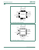
UM10109 Philips Semiconductors P2.0/ICB 1 26 P0.1/CIN2B/KBI1 P2.1/OCD 2 27 P2.6/OCA P0.0/CMP2/KBI0 3 28 P2.7/ICA P1.7/OCC 4 P89LPC932A1 User manual P1.6/OCB 5 25 P0.2/CIN2A/KBI2 P1.5/RST 6 24 P0.3/CIN1B/KBI3 VSS 7 P3.1/XTAL1 8 P3.0/XTAL2/CLKOUT 9 23 P0.4/CIN1A/KBI4 P89LPC932A1FA 22 P0.5/CMPREF/KBI5 21 VDD 20 P0.6/CMP1/KBI6 P1.4/INT1 10 19 P0.7/T1/KBI7 P1.1/RXD 17 P1.0/TXD 18 23 P2.6/OCA 22 P0.1/CIN2B/KBI1 P2.5/SPICLK 16 P2.4/SS 15 P2.3/MISO 14 P2.2/MOSI 13 P1.
UM10109 Philips Semiconductors P89LPC932A1 User manual 1.3 Pin description Table 1: Pin description Symbol Pin Type Description I/O Port 0: Port 0 is an 8-bit I/O port with a user-configurable output type. During reset Port 0 latches are configured in the input only mode with the internal pull-up disabled. The operation of Port 0 pins as inputs and outputs depends upon the port configuration selected. Each port pin is configured independently. Refer to Section 4.
UM10109 Philips Semiconductors P89LPC932A1 User manual Table 1: Pin description …continued Symbol Pin Type Description TSSOP28, HVQFN28 PLCC28 P0.0 to P0.7 (continued) 20 19 16 15 I/O P0.6 — Port 0 bit 6. O CMP1 — Comparator 1 output. I KBI6 — Keyboard input 6. I/O P0.7 — Port 0 bit 7. I/O T1 — Timer/counter 1 external count input or overflow output. I KBI7 — Keyboard input 7. © Koninklijke Philips Electronics N.V. 2005. All rights reserved. User manual Rev.
UM10109 Philips Semiconductors P89LPC932A1 User manual Table 1: Pin description …continued Symbol Pin Type Description TSSOP28, HVQFN28 PLCC28 P1.0 to P1.7 18, 17, 12, 14, 13, 8, 11, 10, 6, 7, 6, 2, 1, 5, 4 28 I/O, I [1] Port 1: Port 1 is an 8-bit I/O port with a user-configurable output type, except for three pins as noted below. During reset Port 1 latches are configured in the input only mode with the internal pull-up disabled.
UM10109 Philips Semiconductors P89LPC932A1 User manual Table 1: Pin description …continued Symbol Pin Type Description I/O Port 2: Port 2 is an 8-bit I/O port with a user-configurable output type. During reset Port 2 latches are configured in the input only mode with the internal pull-up disabled. The operation of Port 2 pins as inputs and outputs depends upon the port configuration selected. Each port pin is configured independently. Refer to Section 4.
UM10109 Philips Semiconductors P89LPC932A1 User manual Table 1: Pin description …continued Symbol Pin Type Description I/O Port 3: Port 3 is a 2-bit I/O port with a user-configurable output type. During reset Port 3 latches are configured in the input only mode with the internal pull-up disabled. The operation of Port 3 pins as inputs and outputs depends upon the port configuration selected. Each port pin is configured independently. Refer to Section 4.
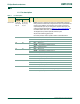
UM10109 Philips Semiconductors P89LPC932A1 User manual P89LPC932A1 ACCELERATED 2-CLOCK 80C51 CPU 8 kB CODE FLASH 256-BYTE DATA RAM UART internal bus 512-BYTE AUXILIARY RAM I2C-BUS SPI REAL-TIME CLOCK/ SYSTEM TIMER 512-BYTE DATA EEPROM TIMER 0 TIMER 1 PORT 3 CONFIGURABLE I/Os ANALOG COMPARATORS PORT 2 CONFIGURABLE I/Os PORT 1 CONFIGURABLE I/Os CCU (CAPTURE/ COMPARE UNIT) PORT 0 CONFIGURABLE I/Os KEYPAD INTERRUPT POWER MONITOR (POWER-ON RESET, BROWNOUT RESET) WATCHDOG TIMER AND OSCILLATOR PROG
UM10109 Philips Semiconductors P89LPC932A1 User manual 1.4 Special function registers Remark: Special Function Registers (SFRs) accesses are restricted in the following ways: • User must not attempt to access any SFR locations not defined. • Accesses to any defined SFR locations must be strictly for the functions for the SFRs.
xxxxxxxxxxxxxxxxxxxxx xxxxxxxxxxxxxxxxxxxxxxxxxx xxxxxxx x x x xxxxxxxxxxxxxxxxxxxxxxxxxxxxxx xxxxxxxxxxxxxxxxxxx xx xx xxxxx xxxxxxxxxxxxxxxxxxxxxxxxxxx xxxxxxxxxxxxxxxxxxx xxxxxx xxxxxxxxxxxxxxxxxxxxxxxxxxxxxxxxxxx xxxxxxxxxxxx x x xxxxxxxxxxxxxxxxxxxxx xxxxxxxxxxxxxxxxxxxxxxxxxxxxxx xxxxx xxxxxxxxxxxxxxxxxxxxxxxxxxxxxxxxxxxxxxxxxxxxxxxxxx xxxxxxxx xxxxxxxxxxxxxxxxxxxxxxxxx xxxxxxxxxxxxxxxxxxxx xxx Philips Semiconductors User manual Table 2: P89LPC932A1 Special function registers * indicates SFRs that
xxxxxxxxxxxxxxxxxxxxx xxxxxxxxxxxxxxxxxxxxxxxxxx xxxxxxx x x x xxxxxxxxxxxxxxxxxxxxxxxxxxxxxx xxxxxxxxxxxxxxxxxxx xx xx xxxxx xxxxxxxxxxxxxxxxxxxxxxxxxxx xxxxxxxxxxxxxxxxxxx xxxxxx xxxxxxxxxxxxxxxxxxxxxxxxxxxxxxxxxxx xxxxxxxxxxxx x x xxxxxxxxxxxxxxxxxxxxx xxxxxxxxxxxxxxxxxxxxxxxxxxxxxx xxxxx xxxxxxxxxxxxxxxxxxxxxxxxxxxxxxxxxxxxxxxxxxxxxxxxxx xxxxxxxx xxxxxxxxxxxxxxxxxxxxxxxxx xxxxxxxxxxxxxxxxxxxx xxx Name Description SFR Bit functions and addresses addr.
xxxxxxxxxxxxxxxxxxxxx xxxxxxxxxxxxxxxxxxxxxxxxxx xxxxxxx x x x xxxxxxxxxxxxxxxxxxxxxxxxxxxxxx xxxxxxxxxxxxxxxxxxx xx xx xxxxx xxxxxxxxxxxxxxxxxxxxxxxxxxx xxxxxxxxxxxxxxxxxxx xxxxxx xxxxxxxxxxxxxxxxxxxxxxxxxxxxxxxxxxx xxxxxxxxxxxx x x xxxxxxxxxxxxxxxxxxxxx xxxxxxxxxxxxxxxxxxxxxxxxxxxxxx xxxxx xxxxxxxxxxxxxxxxxxxxxxxxxxxxxxxxxxxxxxxxxxxxxxxxxx xxxxxxxx xxxxxxxxxxxxxxxxxxxxxxxxx xxxxxxxxxxxxxxxxxxxx xxx Name Description SFR Bit functions and addresses addr. MSB 00 0000 0000 Rev.
xxxxxxxxxxxxxxxxxxxxx xxxxxxxxxxxxxxxxxxxxxxxxxx xxxxxxx x x x xxxxxxxxxxxxxxxxxxxxxxxxxxxxxx xxxxxxxxxxxxxxxxxxx xx xx xxxxx xxxxxxxxxxxxxxxxxxxxxxxxxxx xxxxxxxxxxxxxxxxxxx xxxxxx xxxxxxxxxxxxxxxxxxxxxxxxxxxxxxxxxxx xxxxxxxxxxxx x x xxxxxxxxxxxxxxxxxxxxx xxxxxxxxxxxxxxxxxxxxxxxxxxxxxx xxxxx xxxxxxxxxxxxxxxxxxxxxxxxxxxxxxxxxxxxxxxxxxxxxxxxxx xxxxxxxx xxxxxxxxxxxxxxxxxxxxxxxxx xxxxxxxxxxxxxxxxxxxx xxx Name Description SFR Bit functions and addresses addr.
xxxxxxxxxxxxxxxxxxxxx xxxxxxxxxxxxxxxxxxxxxxxxxx xxxxxxx x x x xxxxxxxxxxxxxxxxxxxxxxxxxxxxxx xxxxxxxxxxxxxxxxxxx xx xx xxxxx xxxxxxxxxxxxxxxxxxxxxxxxxxx xxxxxxxxxxxxxxxxxxx xxxxxx xxxxxxxxxxxxxxxxxxxxxxxxxxxxxxxxxxx xxxxxxxxxxxx x x xxxxxxxxxxxxxxxxxxxxx xxxxxxxxxxxxxxxxxxxxxxxxxxxxxx xxxxx xxxxxxxxxxxxxxxxxxxxxxxxxxxxxxxxxxxxxxxxxxxxxxxxxx xxxxxxxx xxxxxxxxxxxxxxxxxxxxxxxxx xxxxxxxxxxxxxxxxxxxx xxx Name Description SFR Bit functions and addresses addr.
xxxxxxxxxxxxxxxxxxxxx xxxxxxxxxxxxxxxxxxxxxxxxxx xxxxxxx x x x xxxxxxxxxxxxxxxxxxxxxxxxxxxxxx xxxxxxxxxxxxxxxxxxx xx xx xxxxx xxxxxxxxxxxxxxxxxxxxxxxxxxx xxxxxxxxxxxxxxxxxxx xxxxxx xxxxxxxxxxxxxxxxxxxxxxxxxxxxxxxxxxx xxxxxxxxxxxx x x xxxxxxxxxxxxxxxxxxxxx xxxxxxxxxxxxxxxxxxxxxxxxxxxxxx xxxxx xxxxxxxxxxxxxxxxxxxxxxxxxxxxxxxxxxxxxxxxxxxxxxxxxx xxxxxxxx xxxxxxxxxxxxxxxxxxxxxxxxx xxxxxxxxxxxxxxxxxxxx xxx Name Description SFR Bit functions and addresses addr.
UM10109 Philips Semiconductors P89LPC932A1 User manual 1.5 Memory organization FF00h FFEFh 1FFFh read-protected IAP calls only IAP entrypoints IDATA routines entry points for: -51 ASM. code -C code ISP CODE (512B)* 1E00h 1C00h 1BFFh 1800h 17FFh 1400h 13FFh 1000h 0FFFh 0C00h 0BFFh 0800h 07FFh 0400h 03FFh SECTOR 7 SECTOR 4 FF1Fh FF00h entry points SPECIAL FUNCTION REGISTERS (DIRECTLY ADDRESSABLE) IDATA (incl. DATA) 128 BYTES ON-CHIP DATA MEMORY (STACK AND INDIR. ADDR.
UM10109 Philips Semiconductors P89LPC932A1 User manual 2. Clocks 2.1 Enhanced CPU The P89LPC932A1 uses an enhanced 80C51 CPU which runs at six times the speed of standard 80C51 devices. A machine cycle consists of two CPU clock cycles, and most instructions execute in one or two machine cycles. 2.2 Clock definitions The P89LPC932A1 device has several internal clocks as defined below: OSCCLK — Input to the DIVM clock divider.
UM10109 Philips Semiconductors P89LPC932A1 User manual The frequency of this clock output is 1⁄2 that of the CCLK. If the clock output is not needed in Idle mode, it may be turned off prior to entering Idle, saving additional power. Note: on reset, the TRIM SFR is initialized with a factory preprogrammed value. Therefore when setting or clearing the ENCLK bit, the user should retain the contents of other bits of the TRIM register.
UM10109 Philips Semiconductors P89LPC932A1 User manual level. When system power is removed VDD will fall below the minimum specified operating voltage. When using an oscillator frequency above 12 MHz, in some applications, an external brownout detect circuit may be required to hold the device in reset when VDD falls below the minimum specified operating voltage.
UM10109 Philips Semiconductors P89LPC932A1 User manual 2.8 CPU Clock (CCLK) modification: DIVM register The OSCCLK frequency can be divided down, by an integer, up to 510 times by configuring a dividing register, DIVM, to provide CCLK. This produces the CCLK frequency using the following formula: CCLK frequency = fosc / (2N) Where: fosc is the frequency of OSCCLK, N is the value of DIVM. Since N ranges from 0 to 255, the CCLK frequency can be in the range of fosc to fosc/510. (for N = 0, CCLK = fosc).
UM10109 Philips Semiconductors P89LPC932A1 User manual 3.1 Interrupt priority structure Table 6: Interrupt priority level Priority bits IPxH IPx Interrupt priority level 0 0 Level 0 (lowest priority) 0 1 Level 1 1 0 Level 2 1 1 Level 3 There are four SFRs associated with the four interrupt levels: IP0, IP0H, IP1, IP1H. Every interrupt has two bits in IPx and IPxH (x = 0, 1) and can therefore be assigned to one of four levels, as shown in Table 7.
UM10109 Philips Semiconductors P89LPC932A1 User manual Table 7: Summary of interrupts Description Interrupt flag bit(s) Vector address Interrupt enable bit(s) Interrupt priority Arbitration ranking Powerdown wake-up External interrupt 0 IE0 0003h EX0 (IEN0.0) IP0H.0, IP0.0 1 (highest) Yes Timer 0 interrupt TF0 000Bh ET0 (IEN0.1) IP0H.1, IP0.1 4 No External interrupt 1 IE1 0013h EX1 (IEN0.2) IP0H.2, IP0.2 7 Yes Timer 1 interrupt TF1 001Bh ET1 (IEN0.3) IP0H.3, IP0.
UM10109 Philips Semiconductors P89LPC932A1 User manual IE0 EX0 IE1 EX1 BOPD EBO RTCF ERTC (RTCCON.1) WDOVF wake-up (if in power-down) KBIF EKBI EWDRT CMF2 CMF1 EC EA (IE0.7) TF0 ET0 TF1 ET1 TI & RI/RI ES/ESR TI EST interrupt to CPU SI EI2C SPIF ESPI any CCU interrupt (1) ECCU EEIF EIEE 002aaa892 (1) See Section 9 “Capture/Compare Unit (CCU)”. Fig 8. Interrupt sources, interrupt enables, and power-down wake-up sources. 4.
UM10109 Philips Semiconductors P89LPC932A1 User manual 4.1 Port configurations All but three I/O port pins on the P89LPC932A1 may be configured by software to one of four types on a pin-by-pin basis, as shown in Table 9. These are: quasi-bidirectional (standard 80C51 port outputs), push-pull, open drain, and input-only. Two configuration registers for each port select the output type for each port pin. P1.5 (RST) can only be an input and cannot be configured. P1.2 (SCL/T0) and P1.
UM10109 Philips Semiconductors P89LPC932A1 User manual (Please refer to the P89LPC932A1 data sheet, Dynamic characteristics for glitch filter specifications). VDD 2 CPU CLOCK DELAY P P strong very P weak weak PORT PIN port latch data input data glitch rejection 002aaa914 Fig 9. Quasi-bidirectional output. 4.3 Open drain output configuration The open drain output configuration turns off all pull-ups and only drives the pull-down transistor of the port pin when the port latch contains a logic 0.
UM10109 Philips Semiconductors P89LPC932A1 User manual 4.4 Input-only configuration The input port configuration is shown in Figure 11. It is a Schmitt-triggered input that also has a glitch suppression circuit. (Please refer to the P89LPC932A1 data sheet, Dynamic characteristics for glitch filter specifications). input data PORT PIN glitch rejection 002aaa916 Fig 11. Input only. 4.
UM10109 Philips Semiconductors P89LPC932A1 User manual 4.6 Port 0 and Analog Comparator functions The P89LPC932A1 incorporates two Analog Comparators. In order to give the best analog performance and minimize power consumption, pins that are being used for analog functions must have both the digital outputs and digital inputs disabled. Digital outputs are disabled by putting the port pins into the input-only mode as described in the Port Configurations section (see Figure 11).
UM10109 Philips Semiconductors P89LPC932A1 User manual Table 10: Port output configuration …continued Port pin Configuration SFR bits P1.6 PxM1.y PxM2.y P1M1.6 P1M2.6 Alternate usage P1.7 P1M1.7 P1M2.7 P3.0 P3M1.0 P3M2.0 CLKOUT, XTAL2 P3.1 P3M1.1 P3M2.1 XTAL1 Notes 5. Power monitoring functions The P89LPC932A1 incorporates power monitoring functions designed to prevent incorrect operation during initial power-on and power loss or reduction during operation.
UM10109 Philips Semiconductors P89LPC932A1 User manual Table 11: Brownout options[1] BOE (UCFG1.5) PMOD1/ PMOD0 (PCON[1:0]) BOPD (PCON.5) BOI (PCON.4) EBO (IEN0.5) EA (IEN0.7) Description 0 (erased) XX X X X X 1(program med) 11 (total power-down) X X X X Brownout disabled. VDD operating range is 2.4 V to 3.6 V. X X X Brownout disabled. VDD operating range is 2.4 V to 3.6 V. However, BOPD is default to logic 0 upon power-up. X X Brownout reset enabled. VDD operating range is 2.
UM10109 Philips Semiconductors P89LPC932A1 User manual Table 12: Power reduction modes PMOD1 PMOD0 Description (PCON.1) (PCON.0) 0 0 Normal mode (default) - no power reduction. 0 1 Idle mode. The Idle mode leaves peripherals running in order to allow them to activate the processor when an interrupt is generated. Any enabled interrupt source or reset may terminate Idle mode. 1 0 Power-down mode: The Power-down mode stops the oscillator in order to minimize power consumption.
UM10109 Philips Semiconductors P89LPC932A1 User manual Table 13: Power Control register (PCON - address 87h) bit allocation Bit 7 6 5 4 Symbol SMOD1 SMOD0 BOPD Reset 0 0 0 Table 14: 3 2 1 0 BOI GF1 GF0 PMOD1 PMOD0 0 0 0 0 0 Power Control register (PCON - address 87h) bit description Bit Symbol Description 0 PMOD0 Power Reduction Mode (see Section 5.3) 1 PMOD1 2 GF0 General Purpose Flag 0.
UM10109 Philips Semiconductors P89LPC932A1 User manual Table 16: Power Control register A (PCONA - address B5h) bit description …continued Bit Symbol Description 4 - reserved 5 VCPD Analog Voltage Comparators power-down: When logic 1, the voltage comparators are powered down. User must disable the voltage comparators prior to setting this bit. 6 DEEPD Data EEPROM power-down: When logic 1, the Data EEPROM is powered down.
UM10109 Philips Semiconductors P89LPC932A1 User manual • For any other reset, any previously set flag bits that have not been cleared will remain set. RPE (UCFG1.6) RST pin WDTE (UCFG1.7) watchdog timer reset software reset SRST (AUXR1.3) chip reset power-on detect UART break detect EBRR (AUXR1.6) brownout detect reset BOPD (PCON.5) 002aaa918 Fig 13. Block diagram of reset.
UM10109 Philips Semiconductors P89LPC932A1 User manual 6.1 Reset vector Following reset, the P89LPC932A1 will fetch instructions from either address 0000h or the Boot address. The Boot address is formed by using the Boot Vector as the high byte of the address and the low byte of the address = 00h. The Boot address will be used if a UART break reset occurs or the non-volatile Boot Status bit (BOOTSTAT.0) = 1, or the device has been forced into ISP mode.
UM10109 Philips Semiconductors P89LPC932A1 User manual Table 20: Timer/Counter Mode register (TMOD - address 89h) bit description …continued Bit Symbol Description 4 T1M0 5 T1M1 Mode Select for Timer 1. These bits are used with the T1M2 bit in the TAMOD register to determine the Timer 1 mode (see Table 22). 6 T1C/T 7 T1GATE Gating control for Timer 1. When set, Timer/Counter is enabled only while the INT1 pin is high and the TR1 control pin is set.
UM10109 Philips Semiconductors P89LPC932A1 User manual The 13-bit register consists of all 8 bits of THn and the lower 5 bits of TLn. The upper 3 bits of TLn are indeterminate and should be ignored. Setting the run flag (TRn) does not clear the registers. Mode 0 operation is the same for Timer 0 and Timer 1. See Figure 14. There are two different GATE bits, one for Timer 1 (TMOD.7) and one for Timer 0 (TMOD.3). 7.
UM10109 Philips Semiconductors P89LPC932A1 User manual Table 23: Timer/Counter Control register (TCON) - address 88h) bit allocation Bit 7 6 5 4 3 2 1 0 Symbol TF1 TR1 TF0 TR0 IE1 IT1 IE0 IT0 Reset 0 0 0 0 0 0 0 0 Table 24: Timer/Counter Control register (TCON - address 88h) bit description Bit Symbol Description 0 IT0 Interrupt 0 Type control bit. Set/cleared by software to specify falling edge/low level triggered external interrupts. 1 IE0 Interrupt 0 Edge flag.
UM10109 Philips Semiconductors P89LPC932A1 User manual C/T = 0 PCLK Tn pin C/T = 1 overflow TLn (8-bits) control interrupt TFn reload toggle TRn Tn pin gate THn (8-bits) INTn pin ENTn 002aaa921 Fig 16. Timer/counter 0 or 1 in Mode 2 (8-bit auto-reload). C/T = 0 PCLK T0 pin C/T = 1 control overflow TL0 (8-bits) interrupt TF0 toggle TR0 T0 pin (P1.2 open drain) gate INT0 pin ENT0 (AUXR1.4) osc/2 control TH0 (8-bits) overflow interrupt TF1 toggle T1 pin (P0.
UM10109 Philips Semiconductors P89LPC932A1 User manual control bits ENT0 and ENT1 in the AUXR1 register, and apply to Timer 0 and Timer 1 respectively. The port outputs will be a logic 1 prior to the first timer overflow when this mode is turned on. In order for this mode to function, the C/T bit must be cleared selecting PCLK as the clock source for the timer. 8.
UM10109 Philips Semiconductors P89LPC932A1 User manual 8.1 Real-time clock source RTCS1/RTCS0 (RTCCON[6:5]) are used to select the clock source for the RTC if either the Internal RC oscillator or the internal WD oscillator is used as the CPU clock. If the internal crystal oscillator or the external clock input on XTAL1 is used as the CPU clock, then the RTC will use CCLK as its clock source. 8.2 Changing RTCS1/RTCS0 RTCS1/RTCS0 cannot be changed if the RTC is currently enabled (RTCCON.0 = 1).
UM10109 Philips Semiconductors P89LPC932A1 User manual Table 25: Real-time Clock/System Timer clock sources …continued FOSC2:0 RCCLK RTCS1:0 RTC clock source CPU clock source 010 0 00 Low frequency crystal Low frequency crystal /DIVM 01 10 1 11 Low frequency crystal /DIV 00 Low frequency crystal Internal RC oscillator 01 10 011 0 1 100 0 1 11 Internal RC oscillator 00 High frequency crystal 01 Internal RC oscillator Medium frequency crystal /DIVM 10 Low frequency crystal
UM10109 Philips Semiconductors P89LPC932A1 User manual Table 27: Real-time Clock Control register (RTCCON - address D1h) bit description Bit Symbol Description 0 RTCEN Real-time Clock enable. The Real-time Clock will be enabled if this bit is logic 1. Note that this bit will not power-down the Real-time Clock. The RTCPD bit (PCONA.7) if set, will power-down and disable this block regardless of RTCEN. 1 ERTC Real-time Clock interrupt enable.
UM10109 Philips Semiconductors P89LPC932A1 User manual 16-BIT SHADOW REGISTER TOR2H TO TOR2L 16-BIT SHADOW REGISTER OCRxH TO OCRxL 16-BIT COMPARE VALUE OCD OCC OCB TIMER > COMPARE 16-BIT TIMER RELOAD REGISTER OCA COMPARE CHANNELS A TO D OVERFLOW/ UNDERFLOW 16-BIT CAPTURE REGISTER ICRxH, L 16-BIT UP/DOWN TIMER WITH RELOAD EVENT COUNTER FCOx ICNFx ICESx ICB NOISE FILTER EDGE SELECT ICA 10-BIT DIVIDER INTERRUPT FLAG TICF2x SET 4-BIT DIVIDER CAPTURE CHANNELS A, B 002aab009 32 × PLL Fig
UM10109 Philips Semiconductors P89LPC932A1 User manual Up-counting: When the timer contents are FFFFH, the next CCUCLK cycle will set the counter value to the contents of TOR2H:TOR2L. Down-counting: When the timer contents are 0000H, the next CCUCLK cycle will set the counter value to the contents of TOR2H:TOR2L.
UM10109 Philips Semiconductors P89LPC932A1 User manual Table 30: CCU prescaler control register, low byte (TPCR2L - address CAh) bit allocation Bit 7 6 5 4 Symbol TPCR2L.7 TPCR2L.6 TPCR2L.5 Reset 0 0 0 Table 31: Table 32: 3 2 1 0 TPCR2L.4 TPCR2L.3 TPCR2L.2 TPCR2L.1 TPCR2L.0 0 0 0 0 0 CCU prescaler control register, low byte (TPCR2L - address CAh) bit description Bit Symbol Description 0 TPCR2L.0 Prescaler bit 0 1 TPCR2L.1 Prescaler bit 1 2 TPCR2L.
UM10109 Philips Semiconductors P89LPC932A1 User manual will have to set the associated I/O pin to the desired output mode to connect the pin. (Note: The SFR bits for port pins P2.6, P1.6, P1.7, P2.1 must be set to logic 1 in order for the compare channel outputs to be visible at the port pins.) When the contents of TH2:TL2 match that of OCRxH:OCRxL, the Timer Output Compare Interrupt Flag - TOCFx is set in TIFR2. This happens in the CCUCLK cycle after the compare takes place.
UM10109 Philips Semiconductors P89LPC932A1 User manual in basic timer mode. In basic timer mode, writing a one to TCOU2 will cause the values to be latched immediately and the value of TCOU2 will always read as zero. In PWM mode, writing a one to TCOU2 will cause the contents of the shadow registers to be updated on the next CCU Timer overflow. As long as the latch is pending, TCOU2 will read as one and will return to zero when the latch takes place.
UM10109 Philips Semiconductors P89LPC932A1 User manual 9.6 PWM operation PWM Operation has two main modes, asymmetrical and symmetrical. These modes of timer operation are selected by writing 10H or 11H to TMOD21:TMOD20 as shown in Section 9.3 “Basic timer operation”. In asymmetrical PWM operation, the CCU Timer operates in downcounting mode regardless of the setting of TDIR2. In this case, TDIR2 will always read 1.
UM10109 Philips Semiconductors P89LPC932A1 User manual When the timer changes direction at the bottom, in this example, it counts …,0001H, 0000H, 0001H,… The CCU Timer overflow interrupt flag is set in the counter CCUCLK cycle after the transition from 0001H to 0000H. The status of the TDIR2 bit in TCR20 reflects the current counting direction. Writing to this bit while operating in symmetrical mode has no effect. 9.
UM10109 Philips Semiconductors P89LPC932A1 User manual 9.8 Synchronized PWM register update When the OCRx registers are written, a built in mechanism ensures that the value is not updated in the middle of a PWM pulse. This could result in an odd-length pulse. When the registers are written, the values are placed in two shadow registers, as is the case in basic timer operation mode. Writing to TCOU2 will cause the contents of the shadow registers to be updated on the next CCU Timer overflow.
UM10109 Philips Semiconductors P89LPC932A1 User manual Table 39: CCU control register 1 (TCR21 - address F9h) bit description Bit Symbol Description 0:3 PLLDV.3:0 PLL frequency divider. 4:6 - Reserved. 7 In basic timer mode, writing a logic 1 to TCOU2 will cause the values to be latched immediately and the value of TCOU2 will always read as logic 0. In PWM mode, writing a logic 1 to TCOU2 will cause the contents of the shadow registers to be updated on the next CCU Timer overflow.
UM10109 Philips Semiconductors P89LPC932A1 User manual 2. After the current (highest priority) event is serviced, write a logic 0 to the corresponding interrupt flag bit in the TIFR2 register to clear the flag. 3. Read the TISE2 register. If the priority-encoded interrupt source is ‘000’, all CCU interrupts are serviced and a return from interrupt can occur. Otherwise, return to step 2 for the next interrupt. EA (IEN0.7) ECCU (IEN1.4) TOIE2 (TICR2.7) TOIF2 (TIFR2.7) TICIE2A (TICR2.0) TICF2A (TIFR2.
UM10109 Philips Semiconductors P89LPC932A1 User manual Table 41: CCU interrupt status encode register (TISE2 - address DEh) bit description Bit Symbol Description 2:0 ENCINT.2:0 CCU Interrupt Encode output. When multiple interrupts happen, more than one interrupt flag is set in CCU Interrupt Flag Register (TIFR2). The encoder output can be read to determine which interrupt is to be serviced.
UM10109 Philips Semiconductors P89LPC932A1 User manual Table 44: CCU interrupt control register (TICR2 - address C9h) bit allocation Bit 7 6 5 4 3 2 1 0 Symbol TOIE2 TOCIE2D TOCIE2C TOCIE2B TOCIE2A - TICIE2B TICIE2A Reset 0 0 0 0 0 x 0 0 Table 45: CCU interrupt control register (TICR2 - address C9h) bit description Bit Symbol Description 0 TICIE2A Input Capture Channel A Interrupt Enable Bit.
UM10109 Philips Semiconductors P89LPC932A1 User manual 10.3 Mode 2 11 bits are transmitted (through TxD) or received (through RxD): start bit (logic 0), 8 data bits (LSB first), a programmable 9th data bit, and a stop bit (logic 1). When data is transmitted, the 9th data bit (TB8 in SCON) can be assigned the value of 0 or 1. Or, for example, the parity bit (P, in the PSW) could be moved into TB8.
UM10109 Philips Semiconductors P89LPC932A1 User manual 10.7 Updating the BRGR1 and BRGR0 SFRs The baud rate SFRs, BRGR1 and BRGR0 must only be loaded when the Baud Rate Generator is disabled (the BRGEN bit in the BRGCON register is logic 0). This avoids the loading of an interim value to the baud rate generator. (CAUTION: If either BRGR0 or BRGR1 is written when BRGEN = 1, the result is unpredictable.) Table 47: UART baud rate generation SCON.7 (SM0) SCON.6 (SM1) PCON.7 (SMOD1) BRGCON.
UM10109 Philips Semiconductors P89LPC932A1 User manual 10.9 Break detect A break detect is reported in the status register (SSTAT). A break is detected when any 11 consecutive bits are sensed low. Since a break condition also satisfies the requirements for a framing error, a break condition will also result in reporting a framing error. Once a break condition has been detected, the UART will go into an idle state and remain in this idle state until a stop bit has been received.
UM10109 Philips Semiconductors P89LPC932A1 User manual Table 53: Bit Serial Port Status register (SSTAT - address BAh) bit allocation 7 6 5 Symbol DBMOD INTLO CIDIS DBISEL FE BR OE STINT Reset x x x x x x 0 0 Table 54: 4 3 2 1 0 Serial Port Status register (SSTAT - address BAh) bit description Bit Symbol Description 0 STINT Status Interrupt Enable. When set = 1, FE, BR, or OE can cause an interrupt.
UM10109 Philips Semiconductors P89LPC932A1 User manual S1 ... S16 S1 ... S16 S1 ... S16 S1 ... S16 S1 ... S16 S1 ... S16 S1 ... S16 S1 ... S16 S1 ... S16 S1 ... S16 S1 ... S16 S1 ... S16 S1 ... S16 write to SBUF transmit shift RXD (data out) D0 D1 D2 D3 D4 D5 D6 D7 TXD (shift clock) TI WRITE to SCON (clear RI) RI receive shift RXD (data in) TxD (shift clock) D0 D1 D2 D3 D4 D5 D6 D7 002aaa925 Fig 26. Serial Port Mode 0 (double buffering must be disabled). 10.
UM10109 Philips Semiconductors P89LPC932A1 User manual TX clock write to SBUF shift transmit start bit TxD D0 D1 D2 D3 D4 D5 D6 D7 stop bit TI INTLO = 0 RX clock RxD ÷16 reset start bit D0 D1 D2 D3 D4 D5 D6 D7 INTLO = 1 stop bit receive shift RI 002aaa926 Fig 27. Serial Port Mode 1 (only single transmit buffering case is shown). 10.12 More about UART Modes 2 and 3 Reception is the same as in Mode 1.
UM10109 Philips Semiconductors P89LPC932A1 User manual Table 55: FE and RI when SM2= 1 in Modes 2 and 3 Mode PCON.6 (SMOD0) RB8 RI FE 2 0 0 No RI when RB8 = 0 Occurs during STOP bit 1 Similar to Figure 28, with SMOD0 = 0, RI occurs during RB8, one bit before FE Occurs during STOP bit 0 No RI when RB8 = 0 Will NOT occur 3 1 1 [28], with SMOD0 = 1, RI occurs Similar to during STOP bit Occurs during STOP bit 10.
UM10109 Philips Semiconductors P89LPC932A1 User manual – If DBISEL is logic 1 and INTLO is logic 0, a Tx interrupt will occur at the beginning of the STOP bit of the data currently in the shifter (which is also the last data). – If DBISEL is logic 1 and INTLO is logic 1, a Tx interrupt will occur at the end of the STOP bit of the data currently in the shifter (which is also the last data).
UM10109 Philips Semiconductors P89LPC932A1 User manual If double buffering is enabled, TB8 MUST be updated before SBUF is written, as TB8 will be double-buffered together with SBUF data. The operation described in the Section 10.17 “Transmit interrupts with double buffering enabled (Modes 1, 2, and 3)” on page 65 becomes as follows: 1. The double buffer is empty initially. 2. The CPU writes to TB8. 3. The CPU writes to SBUF. 4.
UM10109 Philips Semiconductors P89LPC932A1 User manual 10.20 Automatic address recognition Automatic address recognition is a feature which allows the UART to recognize certain addresses in the serial bit stream by using hardware to make the comparisons. This feature saves a great deal of software overhead by eliminating the need for the software to examine every serial address which passes by the serial port. This feature is enabled by setting the SM2 bit in SCON.
UM10109 Philips Semiconductors P89LPC932A1 User manual interpreting the don’t-cares as ones, the broadcast address will be FF hexadecimal. Upon reset SADDR and SADEN are loaded with 0s. This produces a given address of all ‘don’t cares’ as well as a Broadcast address of all ‘don’t cares’. This effectively disables the Automatic Addressing mode and allows the microcontroller to use standard UART drivers which do not make use of this feature. 11.
UM10109 Philips Semiconductors P89LPC932A1 User manual RP RP SDA I2C-bus SCL P1.3/SDA OTHER DEVICE WITH I2C-BUS INTERFACE P1.2/SCL P89LPC932A1 OTHER DEVICE WITH I2C-BUS INTERFACE 002aaa898 Fig 30. I2C-bus configuration.
UM10109 Philips Semiconductors P89LPC932A1 User manual 11.3 I2C control register The CPU can read and write this register. There are two bits are affected by hardware: the SI bit and the STO bit. The SI bit is set by hardware and the STO bit is cleared by hardware. CRSEL determines the SCL source when the I2C-bus is in master mode. In slave mode this bit is ignored and the bus will automatically synchronize with any clock frequency up to 400 kHz from the master I2C device.
UM10109 Philips Semiconductors P89LPC932A1 User manual Table 62: I2C Control register (I2CON - address D8h) bit description …continued Bit Symbol Description 3 SI I2C Interrupt Flag. This bit is set when one of the 25 possible I2C states is entered. When EA bit and EI2C (IEN1.0) bit are both set, an interrupt is requested when SI is set. Must be cleared by software by writing 0 to this bit. 4 STO STOP Flag. STO = 1: In master mode, a STOP condition is transmitted to the I2C-bus.
UM10109 Philips Semiconductors P89LPC932A1 User manual The values for I2SCLL and I2SCLH do not have to be the same; the user can give different duty cycles for SCL by setting these two registers. However, the value of the register must ensure that the data rate is in the I2C data rate range of 0 to 400 kHz. Thus the values of I2SCLL and I2SCLH have some restrictions and values for both registers greater than three PCLKs are recommended.
UM10109 Philips Semiconductors P89LPC932A1 User manual The first byte transmitted contains the slave address of the receiving device (7 bits) and the data direction bit. In this case, the data direction bit (R/W) will be logic 0 indicating a write. Data is transmitted 8 bits at a time. After each byte is transmitted, an acknowledge bit is received. START and STOP conditions are output to indicate the beginning and the end of a serial transfer.
UM10109 Philips Semiconductors P89LPC932A1 User manual S slave address R A logic 0 = write logic 1 = read DATA A DATA A P data transferred (n Bytes + acknowledge) A = acknowledge (SDA LOW) A = not acknowledge (SDA HIGH) S = START condition from master to slave from slave to master 002aaa930 Fig 32. Format of Master Receiver mode. After a repeated START condition, I2C-bus may switch to the Master Transmitter Mode.
UM10109 Philips Semiconductors P89LPC932A1 User manual S slave address W A logic 0 = write logic 1 = read DATA A DATA A/A P/RS data transferred (n Bytes + acknowledge) A = acknowledge (SDA LOW) A = not acknowledge (SDA HIGH) S = START condition P = STOP condition RS = repeated START condition from master to slave from slave to master 002aaa932 Fig 34. Format of Slave Receiver mode. 11.6.4 Slave Transmitter mode The first byte is received and handled as in the Slave Receiver Mode.
UM10109 Philips Semiconductors P89LPC932A1 User manual 8 I2ADR ADDRESS REGISTER P1.3 COMPARATOR INPUT FILTER P1.3/SDA SHIFT REGISTER OUTPUT STAGE ACK I2DAT BIT COUNTER / ARBITRATION AND SYNC LOGIC INPUT FILTER P1.2/SCL SERIAL CLOCK GENERATOR OUTPUT STAGE CCLK TIMING AND CONTROL LOGIC interrupt INTERNAL BUS 8 timer 1 overflow P1.2 I2CON I2SCLH I2SCLL CONTROL REGISTERS AND SCL DUTY CYCLE REGISTERS 8 status bus I2STAT STATUS DECODER STATUS REGISTER 8 002aaa899 Fig 36.
UM10109 Philips Semiconductors P89LPC932A1 User manual Table 68: Master Transmitter mode Status code (I2STAT) Status of the I2C hardware Next action taken by I2C hardware Application software response to/from I2DAT to I2CON STA STO SI AA 08H A START condition has been transmitted Load SLA+W x 0 0 x SLA+W will be transmitted; ACK bit will be received 10H A repeat START condition has been transmitted Load SLA+W or x 0 0 x As above; SLA+W will be transmitted; I2C-bus switches to Mas
UM10109 Philips Semiconductors P89LPC932A1 User manual Table 68: Master Transmitter mode …continued Status code (I2STAT) Status of the I2C hardware to/from I2DAT to I2CON STA 30h Data byte in I2DAT Load data byte or 0 has been transmitted, NOT no I2DAT action or 1 ACK has been received no I2DAT action or 0 38H Table 69: Arbitration lost in SLA+R/W or data bytes Next action taken by I2C hardware Application software response STO SI AA 0 0 x Data byte will be transmitted; ACK bit will be
UM10109 Philips Semiconductors P89LPC932A1 User manual Table 69: Master Receiver mode …continued Status code (I2STAT) 50h 58h Table 70: Status of the I2C hardware to/from I2DAT to I2CON STA STO SI STA Data byte has been received; ACK has been returned Read data byte 0 0 0 0 Data byte will be received; NOT ACK bit will be returned read data byte 0 0 0 1 Data byte will be received; ACK bit will be returned Data byte has been received; NACK has been returned Read data byte or 1 0 0
UM10109 Philips Semiconductors P89LPC932A1 User manual Table 70: Slave Receiver mode …continued Status code (I2STAT) Status of the I2C hardware to/from I2DAT to I2CON STA 88H Next action taken by I2C hardware Application software response STO SI AA 0 0 0 Switched to not addressed SLA mode; no recognition of own SLA or general address 0 0 1 Switched to not addressed SLA mode; Own SLA will be recognized; general call address will be recognized if I2ADR.
UM10109 Philips Semiconductors P89LPC932A1 User manual Table 70: Slave Receiver mode …continued Status code (I2STAT) A0H Table 71: B0h B8H Next action taken by I2C hardware Application software response to/from I2DAT to I2CON STA STO SI AA A STOP condition No I2DAT action or repeated START condition has been received no I2DAT action while still addressed as SLA/REC or SLA/TRX no I2DAT action 0 0 0 0 Switched to not addressed SLA mode; no recognition of own SLA or General call address 0
UM10109 Philips Semiconductors P89LPC932A1 User manual Table 71: Slave Transmitter mode …continued Status code (I2STAT) C0H C8H Status of the I2C hardware Application software response Next action taken by I2C to/from I2DAT hardware to I2CON STA STO SI AA 0 0 0 0 Switched to not addressed SLA mode; no recognition of own SLA or General call address.
UM10109 Philips Semiconductors P89LPC932A1 User manual S M CPU clock 8-BIT SHIFT REGISTER MSTR SPR0 SS P2.4 SPR0 SPR1 CPOL CPHA MSTR SSIG DORD MSTR SPEN SPEN SPR1 SPIF S M CLOCK LOGIC SPEN SPI clock (master) WCOL SPICLK P2.5 clock SELECT SPI CONTROL MOSI P2.2 PIN CONTROL LOGIC READ DATA BUFFER DIVIDER BY 4, 16, 64, 128 MISO P2.3 M S SPI CONTROL REGISTER SPI STATUS REGISTER SPI interrupt request internal data bus 002aaa900 Fig 37. SPI block diagram.
UM10109 Philips Semiconductors P89LPC932A1 User manual Table 73: SPI Control register (SPCTL - address E2h) bit description Bit Symbol Description 0 SPR0 SPI Clock Rate Select 1 SPR1 SPR1, SPR0: 00 — CCLK⁄4 01 — CCLK⁄16 10 — CCLK⁄64 11 — CCLK⁄128 2 CPHA SPI Clock PHAse select (see Figure 41 to Figure 44): 1 — Data is driven on the leading edge of SPICLK, and is sampled on the trailing edge.
UM10109 Philips Semiconductors P89LPC932A1 User manual Table 76: Bit SPI Data register (SPDAT - address E3h) bit allocation 7 Symbol MSB Reset 0 6 5 4 3 2 1 0 0 0 0 0 0 0 0 LSB master 8-BIT SHIFT REGISTER slave MISO MISO MOSI MOSI SPICLK SPI CLOCK GENERATOR PORT 8-BIT SHIFT REGISTER SPICLK SS 002aaa901 Fig 38. SPI single master single slave configuration. In Figure 38, SSIG (SPCTL.7) for the slave is logic 0, and SS is used to select the slave.
UM10109 Philips Semiconductors P89LPC932A1 User manual master slave 8-BIT SHIFT REGISTER MISO MISO MOSI MOSI SPICLK SPI CLOCK GENERATOR 8-BIT SHIFT REGISTER SPICLK SS port slave MISO MOSI 8-BIT SHIFT REGISTER SPICLK port SS 002aaa903 Fig 40. SPI single master multiple slaves configuration. In Figure 40, SSIG (SPCTL.7) bits for the slaves are logic 0, and the slaves are selected by the corresponding SS signals. The SPI master can use any port pin (including P2.4/SS) to drive the SS pins.
UM10109 Philips Semiconductors P89LPC932A1 User manual Table 77: SPI master and slave selection …continued SPEN SSIG SS Pin MSTR 1 0 1 1 Master MISO or Slave Mode MOSI SPICLK Remarks Master Hi-Z Hi-Z MOSI and SPICLK are at high-impedance to avoid bus contention when the MAster is idle. The application must pull-up or pull-down SPICLK (depending on CPOL - SPCTL.3) to avoid a floating SPICLK. output output MOSI and SPICLK are push-pull when the Master is active.
UM10109 Philips Semiconductors P89LPC932A1 User manual slave and start sending data to it. To avoid bus contention, the SPI becomes a slave. As a result of the SPI becoming a slave, the MOSI and SPICLK pins are forced to be an input and MISO becomes an output. The SPIF flag in SPSTAT is set, and if the SPI interrupt is enabled, an SPI interrupt will occur. User software should always check the MSTR bit.
UM10109 Philips Semiconductors P89LPC932A1 User manual 1 clock cycle 2 3 4 5 6 7 8 SPICLK (CPOL = 0) SPICLK (CPOL = 1) MOSI (input) MISO (output) DORD = 0 MSB 6 5 4 3 2 1 LSB DORD = 1 LSB 1 2 3 4 5 6 MSB DORD = 0 MSB 6 5 4 3 2 1 LSB DORD = 1 LSB 1 2 3 4 5 6 MSB (1) SS (if SSIG bit = 0) 002aaa934 (1) Not defined Fig 41. SPI slave transfer format with CPHA = 0. © Koninklijke Philips Electronics N.V. 2005. All rights reserved. User manual Rev.
UM10109 Philips Semiconductors P89LPC932A1 User manual 1 clock cycle 2 3 4 5 6 7 8 SPICLK (CPOL = 0) SPICLK (CPOL = 1) MOSI (input) MISO (output) DORD = 0 MSB 6 5 4 3 2 1 LSB DORD = 1 LSB 1 2 3 4 5 6 MSB MSB 6 5 4 3 2 1 LSB LSB 1 2 3 4 5 6 MSB DORD = 0 DORD = 1 (1) SS (if SSIG bit = 0) 002aaa935 (1) Not defined Fig 42. SPI slave transfer format with CPHA = 1. © Koninklijke Philips Electronics N.V. 2005. All rights reserved. User manual Rev.
UM10109 Philips Semiconductors P89LPC932A1 User manual 1 clock cycle 2 3 4 5 6 7 8 SPICLK (CPOL = 0) SPICLK (CPOL = 1) MOSI (input) DORD = 0 MSB 6 5 4 3 2 1 LSB DORD = 1 LSB 1 2 3 4 5 6 MSB MISO (output) DORD = 0 MSB 6 5 4 3 2 1 LSB DORD = 1 LSB 1 2 3 4 5 6 MSB SS (if SSIG bit = 0) 002aaa936 (1) Not defined Fig 43. SPI master transfer format with CPHA = 0. © Koninklijke Philips Electronics N.V. 2005. All rights reserved. User manual Rev.
UM10109 Philips Semiconductors P89LPC932A1 User manual 1 Clock cycle 2 3 4 5 6 7 8 SPICLK (CPOL = 0) SPICLK (CPOL = 1) MOSI (input) MISO (output) DORD = 0 MSB 6 5 4 3 2 1 LSB DORD = 1 LSB 1 2 3 4 5 6 MSB DORD = 0 MSB 6 5 4 3 2 1 LSB DORD = 1 LSB 1 2 3 4 5 6 MSB SS (if SSIG bit = 0) 002aaa937 (1) Not defined Fig 44. SPI master transfer format with CPHA = 1. 12.
UM10109 Philips Semiconductors P89LPC932A1 User manual When each comparator is first enabled, the comparator output and interrupt flag are not guaranteed to be stable for 10 microseconds. The corresponding comparator interrupt should not be enabled during that time, and the comparator interrupt flag must be cleared before the interrupt is enabled in order to prevent an immediate interrupt service.
UM10109 Philips Semiconductors P89LPC932A1 User manual 13.2 Internal reference voltage An internal reference voltage, Vref, may supply a default reference when a single comparator input pin is used. Please refer to the P89LPC932A1 data sheet for specifications 13.3 Comparator input pins Comparator input and reference pins maybe be used as either digital I/O or as inputs to the comparator. When used as digital I/O these pins are 5 V tolerant.
UM10109 Philips Semiconductors P89LPC932A1 User manual CINnA CINnA COn CMPREF 002aaa618 CMPn 002aaa620 a. CPn, CNn, OEn = 0 0 0 b. CPn, CNn, OEn = 0 0 1 CINnA CINnA COn VREF (1.23 V) COn CMPn VREF (1.23 V) 002aaa621 002aaa622 c. CPn, CNn, OEn = 0 1 0 d. CPn, CNn, OEn = 0 1 1 CINnB CINnB COn CMPREF COn CMPREF 002aaa623 CMPn 002aaa624 e. CPn, CNn, OEn = 1 0 0 f. CPn, CNn, OEn = 1 0 1 CINnB CINnB COn VREF (1.23V) COn CMPREF 002aaa625 g. CPn, CNn, OEn = 1 1 0 COn CMPn VREF (1.
UM10109 Philips Semiconductors P89LPC932A1 User manual 14. Keypad interrupt (KBI) The Keypad Interrupt function is intended primarily to allow a single interrupt to be generated when Port 0 is equal to or not equal to a certain pattern. This function can be used for bus address recognition or keypad recognition. The user can configure the port via SFRs for different tasks. There are three SFRs used for this function.
UM10109 Philips Semiconductors P89LPC932A1 User manual Table 84: Keypad Interrupt Mask register (KBMASK - address 86h) bit allocation Bit 7 Symbol KBMASK.7 KBMASK.6 Reset 0 0 Table 85: 6 5 4 3 2 1 0 KBMASK.5 KBMASK.4 KBMASK.3 KBMASK.2 KBMASK.1 KBMASK.0 0 0 0 0 0 0 Keypad Interrupt Mask register (KBMASK - address 86h) bit description Bit Symbol Description 0 KBMASK.0 When set, enables P0.0 as a cause of a Keypad Interrupt. 1 KBMASK.1 When set, enables P0.
UM10109 Philips Semiconductors P89LPC932A1 User manual Figure 49 shows the watchdog timer in watchdog mode. It consists of a programmable 13-bit prescaler, and an 8-bit down counter. The down counter is clocked (decremented) by a tap taken from the prescaler. The clock source for the prescaler is either PCLK or the watchdog oscillator selected by the WDCLK bit in the WDCON register. (Note that switching of the clock sources will not take effect immediately - see Section 15.3).
UM10109 Philips Semiconductors P89LPC932A1 User manual these two SFRs will not take effect. To avoid a watchdog reset, the watchdog timer needs to be fed (via a special sequence of software action called the feed sequence) prior to reaching an underflow. To feed the watchdog, two write instructions must be sequentially executed successfully. Between the two write instructions, SFR reads are allowed, but writes are not allowed.
UM10109 Philips Semiconductors P89LPC932A1 User manual The maximum number of tclks is: tclks = ( 2 (5 + 7) ) ( 255 + 1 ) + 1 = 1048577 (3) Table 89 shows sample P89LPC932A1 timeout values.
UM10109 Philips Semiconductors P89LPC932A1 User manual Table 89: Watchdog timeout vales …continued PRE2 to PRE0 110 111 WDL in decimal) Timeout Period Watchdog Clock Source (in watchdog clock cycles) 400 KHz Watchdog Oscillator Clock (Nominal) 12 MHz CCLK (6 MHz CCLK⁄ Watchdog 2 Clock) 0 2,049 5.12 ms 341.5 µs 255 524,289 1.31 s 87.4 ms 0 4097 10.2 ms 682.8 µs 255 1,048,577 2.62 s 174.8 ms 15.3 Watchdog clock source The watchdog timer system has an on-chip 400 KHz oscillator.
UM10109 Philips Semiconductors P89LPC932A1 User manual WDL (C1H) MOV WFEED1, #0A5H MOV WFEED2, #05AH watchdog oscillator PCLK ÷32 8-BIT DOWN COUNTER PRESCALER reset (1) SHADOW REGISTER WDCON (A7H) PRE2 PRE1 PRE0 - - WDRUN WDTOF WDCLK 002aaa905 Fig 48. Watchdog Timer in Watchdog Mode (WDTE = 1). 15.4 Watchdog Timer in Timer mode Figure 49 shows the Watchdog Timer in Timer Mode. In this mode, any changes to WDCON are written to the shadow register after one watchdog clock cycle.
UM10109 Philips Semiconductors P89LPC932A1 User manual 15.5 Power-down operation The WDT oscillator will continue to run in power-down, consuming approximately 50 µA, as long as the WDT oscillator is selected as the clock source for the WDT. Selecting PCLK as the WDT source will result in the WDT oscillator going into power-down with the rest of the device (see Section 15.3). Power-down mode will also prevent PCLK from running and therefore the watchdog is effectively disabled. 15.
UM10109 Philips Semiconductors P89LPC932A1 User manual 16.1 Software reset The SRST bit in AUXR1 gives software the opportunity to reset the processor completely, as if an external reset or watchdog reset had occurred. If a value is written to AUXR1 that contains a 1 at bit position 3, all SFRs will be initialized and execution will resume at program address 0000. Care should be taken when writing to AUXR1 to avoid accidental software resets. 16.
UM10109 Philips Semiconductors P89LPC932A1 User manual Table 92: Bit Data EEPROM control register (DEECON address F1h) bit allocation 7 6 5 4 3 2 1 0 Symbol EEIF HVERR ECTL1 ECTL0 - - - EADR8 Reset 0 0 0 0 0 0 x 0 Table 93: Data EEPROM control register (DEECON address F1h) bit description Bit Symbol Description 0 Most significant address (bit 8) of the Data EEPROM. EADR7-0 are in DEEADR. EADR8 1:3 Reserved.
UM10109 Philips Semiconductors P89LPC932A1 User manual Note that if DEEDAT is written prior to a write to DEEADR (if DEECON[5:4] = ‘00’), a Data EEPROM write operation will commence. The user must take caution that such cases do not occur during a read. An example is if the Data EEPROM is read in an interrupt service routine with the interrupt occurring in the middle of a Data EEPROM cycle. The user should disable interrupts during a Data EEPROM write operation (see Section 17.2). 17.
UM10109 Philips Semiconductors P89LPC932A1 User manual 1. Write to DEECON with ECTL1/ECTL0 (DEECON[5:4]) = ‘10’ and correct bit 8 address to EADR8. (Note that if the correct values are already written to DEECON, there is no need to write to this register.) 2. Write the fill pattern to the DEEDAT register. (Note that if the correct values are already written to DEEDAT, there is no need to write to this register.) 3. Write address bits 7 to 0 to DEEADR. Note that address bits 5 to 0 are ignored. 4.
UM10109 Philips Semiconductors P89LPC932A1 User manual • Internal fixed boot ROM, containing low-level In-Application Programming (IAP) routines that can be called from the end application (in addition to IAP-Lite). • Default serial loader providing In-System Programming (ISP) via the serial port, located in upper end of user program memory. • Boot vector allows user provided Flash loader code to reside anywhere in the Flash memory space, providing flexibility to the user.
UM10109 Philips Semiconductors P89LPC932A1 User manual • FMADRL, FMADRH (Flash memory address low, Flash memory address high). Used to specify the byte address within the page register or specify the page within user code memory • FMDATA (Flash Data Register). Accepts data to be loaded into the page register. The page register consists of 64 bytes and an update flag for each byte. When a LOAD command is issued to FMCON the page register contents and all of the update flags will be cleared.
UM10109 Philips Semiconductors P89LPC932A1 User manual • Write the address of the next byte to be programmed to FMADRL, if desired. (Not needed for contiguous bytes since FMADRL is auto-incremented). All bytes to be programmed must be within the same page. • Write the data for the next byte to be programmed to FMDATA. • Repeat writing of FMADRL and/or FMDATA until all desired bytes have been loaded into the page register.
UM10109 Philips Semiconductors P89LPC932A1 User manual ;* R5 = page address LSB(byte) * ;* R7 = pointer to data buffer in RAM(byte) * ;* Outputs: * ;* R7 = status (byte) * ;* C = clear on no error, set on error * ;************************************************** LOAD EP EQU EQU 00H 68H PGM_USER: MOV FMCON,#LOAD MOV FMADRH,R4 MOV FMADRL,R5 MOV A,R7 MOV R0,A LOAD_PAGE: MOV FMDAT,@R0 INC R0 DJNZ R3,LOAD_PAGE MOV FMCON,#EP ;load command, clears page register ;get high address ;get low address ; ;get po
UM10109 Philips Semiconductors P89LPC932A1 User manual FMCON = LOAD; //load command, clears page reg FMADRH = page_hi; // FMADRL = page_lo; //write my page address to addr regs for (i=0;i<64;i=i+1) { FMDATA = dbytes[i]; } FMCON = EP; //erase & prog page command Fm_stat = FMCON; //read the result status if ((Fm_stat & 0x0F)!=0) prog_fail=1; else prog_fail=0; return(prog_fail); } 18.5 In-circuit programming (ICP) (This feature was not present in the original P89LPC932).
UM10109 Philips Semiconductors P89LPC932A1 User manual 18.8 Power on reset code execution The P89LPC932A1 contains two special Flash elements: the BOOT VECTOR and the Boot Status Bit. Following reset, the P89LPC932A1 examines the contents of the Boot Status Bit. If the Boot Status Bit is set to zero, power-up execution starts at location 0000H, which is the normal start address of the user’s application code.
UM10109 Philips Semiconductors P89LPC932A1 User manual 18.10 In-system programming (ISP) In-System Programming is performed without removing the microcontroller from the system. The In-System Programming facility consists of a series of internal hardware resources coupled with internal firmware to facilitate remote programming of the P89LPC932A1 through the serial port. This firmware is provided by Philips and embedded within each P89LPC932A1 device.
UM10109 Philips Semiconductors P89LPC932A1 User manual Table 97: In-system Programming (ISP) hex record formats Record type 00 Command/data function Program User Code Memory Page :nnaaaa00dd..ddcc Where: nn = number of bytes to program aaaa = page address dd..
UM10109 Philips Semiconductors P89LPC932A1 User manual Table 97: In-system Programming (ISP) hex record formats …continued Record type Command/data function 03 Miscellaneous Read Functions :01xxxx03sscc Where xxxx = required field but value is a ‘don’t care’ ss= subfunction code cc = checksum Subfunction codes: 00= UCFG1 01= reserved 02= Boot Vector 03= Status Byte 04= reserved 05= reserved 06= reserved 07= reserved 08= Security Byte 0 09= Security Byte 1 0A= Security Byte 2 0B= Security Byte 3 0C=
UM10109 Philips Semiconductors P89LPC932A1 User manual Table 97: In-system Programming (ISP) hex record formats …continued Record type Command/data function 05 Read Sector CRC :01xxxx05aacc Where: xxxx = required field but value is a ‘don’t care’ aa= sector address high byte cc= checksum Example: :0100000504F6cc 06 Read Global CRC :00xxxx06cc Where: xxxx = required field but value is a ‘don’t care’ cc= checksum Example: :00000006FA 07 Direct Load of Baud Rate :02xxxx07HHLLcc Where: xxxx = requir
UM10109 Philips Semiconductors P89LPC932A1 User manual IAP functions which write or erase code memory require an authorization key be set by the calling routine prior to performing the IAP function call. This authorization key is set by writing 96H to RAM location FFH. The following example was written using the Keil C compiler. The methods used to access a specific physical address in memory may vary with other compilers. #include
UM10109 Philips Semiconductors P89LPC932A1 User manual If the Configuration Write Protect bit (CWP) in BOOTSTAT.6 is a logic 1, writes to the configuration bytes are disabled. If the Configuration Write Protect bit (CWP) is a logic 0, writes to the configuration bytes are enabled. The CWP bit is set by programming the BOOTSTAT register. This bit is cleared by using the Clear Configuration Protection (CCP) command in IAP or ISP.
UM10109 Philips Semiconductors P89LPC932A1 User manual Table 99: IAP function calls IAP function IAP call parameters Program User Code Page (requires ‘key’) Input parameters: ACC = 00h R3= number of bytes to program R4= page address (MSB) R5= page address (LSB) R7= pointer to data buffer in RAM F1= 0h = use IDATA Return parameter(s): R7= status Carry= set on error, clear on no error Read Version Id Input parameters: ACC = 01h Return parameter(s): R7= IAP code version id Misc.
UM10109 Philips Semiconductors P89LPC932A1 User manual Table 99: IAP function calls …continued IAP function IAP call parameters Misc.
UM10109 Philips Semiconductors P89LPC932A1 User manual Table 99: IAP function calls …continued IAP function IAP call parameters Read Sector CRC Input parameters: ACC = 05h R7= sector address Return parameter(s): R4= CRC bits 31:24 R5= CRC bits 23:16 R6= CRC bits 15:8 R7= CRC bits 7:0 (if no error) R7= error status (if error) Carry= set on error, clear on no error Read Global CRC Input parameters: ACC = 06h Return parameter(s): R4= CRC bits 31:24 R5= CRC bits 23:16 R6= CRC bits 15:8 R7= CRC bits 7:
UM10109 Philips Semiconductors P89LPC932A1 User manual Table 101: Flash User Configuration Byte (UCFG1) bit description …continued Bit Symbol Description 4 WDSE Watchdog Safety Enable bit. Refer to Table 86 “Watchdog timer configuration” for details. 5 BOE Brownout Detect Enable (see Section 5.1 “Brownout detection”) 6 RPE Reset pin enable. When set = 1, enables the reset function of pin P1.5. When cleared, P1.5 may be used as an input pin.
UM10109 Philips Semiconductors P89LPC932A1 User manual Table 105: Effects of Security Bits EDISx SPEDISx MOVCDISx Effects on Programming 0 0 0 None. 0 0 1 Security violation flag set for sector CRC calculation for the specific sector. Security violation flag set for global CRC calculation if any MOVCDISx bit is set. Cycle aborted. Memory contents unchanged. CRC invalid. Program/erase commands will not result in a security violation.
UM10109 Philips Semiconductors P89LPC932A1 User manual Table 109: Boot Status (BOOTSTAT) bit description …continued Bit Symbol Description 5 AWP Activate Write Protection bit. When this bit is cleared, the internal Write Enable flag is forced to the set state, thus writes to the flash memory are always enabled. When this bit is set, the Write Enable internal flag can be set or cleared using the Set Write Enable (SWE) or Clear Write Enable (CWE) commands. 6 CWP Configuration Write Protect bit.
UM10109 Philips Semiconductors P89LPC932A1 User manual 19.
UM10109 Philips Semiconductors P89LPC932A1 User manual Table 110: Instruction set summary …continued Mnemonic Description Bytes Cycles Hex code ORL A,@Ri OR indirect memory to A 1 1 46 to 47 ORL A,#data OR immediate to A 2 1 44 ORL dir,A OR A to direct byte 2 1 42 ORL dir,#data OR immediate to direct byte 3 2 43 XRL A,Rn Exclusive-OR register to A 1 1 68 to 6F XRL A,dir Exclusive-OR direct byte to A 2 1 65 XRL A, @Ri Exclusive-OR indirect memory to 1 A 1 66 to 67 XR
UM10109 Philips Semiconductors P89LPC932A1 User manual Table 110: Instruction set summary …continued Mnemonic Description Bytes Cycles Hex code MOVX A,@Ri Move external data(A8) to A 1 2 E2 to E3 MOVX A,@DPTR Move external data(A16) to A 1 2 E0 MOVX @Ri,A Move A to external data(A8) 1 2 F2 to F3 MOVX @DPTR,A Move A to external data(A16) 1 2 F0 PUSH dir Push direct byte onto stack 2 2 C0 POP dir Pop direct byte from stack 2 2 D0 XCH A,Rn Exchange A and register 1 1 C
UM10109 Philips Semiconductors P89LPC932A1 User manual Table 110: Instruction set summary …continued Mnemonic Description Bytes Cycles Hex code JZ rel Jump on accumulator = 0 2 2 60 JNZ rel Jump on accumulator ≠ 0 2 2 70 CJNE A,dir,rel Compare A, direct jne relative 3 2 B5 CJNE A,#d,rel Compare A, immediate jne relative 3 2 B4 CJNE Rn,#d,rel Compare register, immediate jne 3 relative 2 B8 to BF CJNE @Ri,#d,rel Compare indirect, immediate jne 3 relative 2 B6 to B7 DJNZ Rn,
UM10109 Philips Semiconductors P89LPC932A1 User manual 20. Disclaimers Life support — These products are not designed for use in life support appliances, devices, or systems where malfunction of these products can reasonably be expected to result in personal injury. Philips Semiconductors customers using or selling these products for use in such applications do so at their own risk and agree to fully indemnify Philips Semiconductors for any damages resulting from such application.
UM10109 Philips Semiconductors P89LPC932A1 User manual 22. Contents 1 Introduction . . . . . . . . . . . . . . . . . . . . . . . . . . . . 3 1.1 Comparison to the P89LPC932 device. . . . . . . 3 1.1.1 Byte-erasability (IAP-Lite) . . . . . . . . . . . . . . . . . 3 1.1.2 Serial in-circuit programming (ICP). . . . . . . . . . 3 1.1.3 ‘On-the-fly’ clock selection . . . . . . . . . . . . . . . . 3 1.1.4 Increased ISP/IAP functionality . . . . . . . . . . . . 4 1.1.4.1 Support for the watchdog timer. . . . .
UM10109 Philips Semiconductors P89LPC932A1 User manual 10.17 10.18 10.19 10.20 11 11.1 11.2 11.3 11.4 11.5 11.6 11.6.1 11.6.2 11.6.3 11.6.4 12 12.1 12.2 12.3 12.4 12.5 12.6 12.7 13 13.1 13.2 13.3 13.4 13.5 13.6 14 15 15.1 15.2 15.3 15.4 15.5 15.6 16 16.1 16.2 17 17.1 17.2 17.3 Transmit interrupts with double buffering enabled (Modes 1, 2, and 3) . . . . . . . . . . . . . . . . . . . . 65 The 9th bit (bit 8) in double buffering (Modes 1, 2, and 3) . . . . . . . . . . . . . . . . . . . . . . . . . . . . .