
Data Sheet

AV6301 Datasheet (Preliminary) revision 0.2
CONTENTS SUBJECT TO CHANGE WITHOUT NOTICE 12 AVNERA PROPRIETARY & CONFIDENTIAL | PROVIDED UNDER NDA
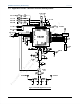
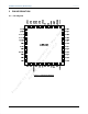
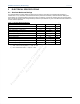
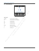
Pin No. Symbol Pin Type Description
PWM2 PWM resource #2
38 VDDDIG Bypass Bypass capacitor pin for 1.35V digital core regulator
39 VDD18 Bypass Bypass capacitor pin for 1.8V digital regulator (LDO)
40 VDDIO Bypass Bypass capacitor pin for 3.3V digital I/O regulator
41 DM USB I/O USB negative input
42 DP USB I/O USB positive input
43 GPIO18
PWM1
GPIO port 18, usage is programmable to GPIO OR to
PWM resource #1
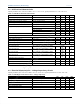
44 GPIO5
S_MISO (SPI Slave)
S_SCL (TWI Slave)
Digital I/O GPIO port 5; usage is programmable to GPIO OR to
S_MISO OR to
S_SCL
45 GPIO4
S_MOSI (SPI Slave)
S_SDA (TWI Slave)
Digital I/O GPIO port 4; usage is programmable to GPIO OR to
S_MOSI OR to
S_SDA
46 GPIO3
S_SCLK (SPI Slave)
UART_RX
PWM1
Digital I/O GPIO port 3; usage is programmable to GPIO OR to
S_SCLK OR to
The UART Receiver OR to
PWM resource #1
47 GPIO2
S_SSB (SPI Slave)
UART_TX
PWM0
Digital I/O GPIO port 2; usage is programmable to GPIO OR to
S_SSB OR to
The UART Transmitter OR to
PWM resource #0
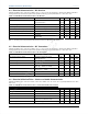
48 GPIO17
PWM2
Digital I/O GPIO port 17, usage is programmable to GPIO OR to
PWM resource #2