
Data Sheet

AV6301 Datasheet (Preliminary) revision 0.2
CONTENTS SUBJECT TO CHANGE WITHOUT NOTICE 11 AVNERA PROPRIETARY & CONFIDENTIAL | PROVIDED UNDER NDA
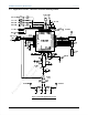
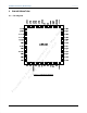
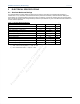
2.2 Pin Description
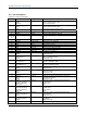
Table 2-2-1 AV301 pin description
Pin No. Symbol Pin Type Description
1 GPIO1
DSCN
DPA-EN
Digital Output GPIO port 1; Usage is programmable to GPIO OR to
Antenna Diversity Switch – OR to
Power Amplifier Enable
2 GPIO0
DSCP
DSC
Digital Output GPIO port 0; Usage is programmable to GPIO OR to
Antenna Diversity Switch + OR to
Single Polarity Diversity Switch Control
3 XTALP Analog input External crystal input
4 XTALN Analog input External crystal input
5 VDDXO Analog Crystal oscillator regulator bypass pin
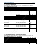
6,8,10-14,
16, 19, 20,
23
N/C - No connection – Leave unconnected – Do not Ground
7 IREF Analog pin Reference current setting resistor connection
9 BGOUT Analog bypass Bandgap reference bypass pin
15 VDDRXADC Bypass Bypass pin for Receiver Data Converter Supply
17 RFP RF I/O RF input/output positive
18 RFN RF I/O RF input/output negative
21 VDC Supply pin 5V input supply voltage from USB
22 V3P6 Bypass Bypass pin for 3.6V main regulator
24 RESETN Digital input RESET signal; active low
25 GPIO16
PWM2
Digital I/O GPIO port 16, usage is programmable to GPIO OR to
PWM resource #2
26 GPIO15
I2S MONO OUT
PWM1
Digital I/O GPIO port 15, usage is programmable to GPIO OR to
I2S port 2 MONO OUT Data
PWM resource #1
27 GPIO14
I2S STEREO IN
Digital I/O GPIO port 14; usage is programmable to GPIO OR to
I2S Port 1 STEREO IN Data
28 GPIO13
I2S STEREO OUT
Digital I/O GPIO port 13; usage is programmable to GPIO OR to
I2S Port 0 STEREO OUT Data
29 GPIO12
WCLK
Digital I/O GPIO port 12; usage is programmable to GPIO OR to
I2S Word Clock
30 GPIO11
BCLK
PWM1
Digital I/O GPIO port 11; usage is programmable to GPIO OR to
I2S Bit Clock OR to
PWM resource #1
32 VDDIO Supply Supply bypass capacitor pin for digital I/O
31 GPIO10
MCLK
PWM0
Digital I/O GPIO port 10; usage is programmable to GPIO OR to
I2S Master Clock OR to
PWM resource #0
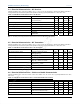
33 GPIO9
M_MISO (SPI Mater)
M_SCL (TWI Master)
SCL (TWI)
Digital I/O GPIO port 9; usage is programmable to GPIO OR to
M_MISO OR to
M_SCL OR to
SCL
34 GPIO8
M_MOSI (SPI Master)
M_SDA (TWI Master)
SDA (TWI)
Digital I/O GPIO port 8; usage is programmable to GPIO OR to
M-MOSI OR to
M_SDA OR to
SDA
35 GPIO7
M_SCLK (SPI Master)
PWM1
Digital I/O GPIO port 7; usage is programmable to GPIO OR to
M_SCLK OR to
PWM resource #1
36 GPIO6
M_SSB (SPI Master)
PWM0
Digital I/O GPIO port 6; usage is programmable to GPIO OR to
M-SSB OR to
PWM resource #0
37 GPIO19 Digital I/O GPIO port 19, usage is programmable to GPIO OR to