
Datasheet
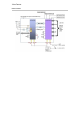
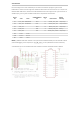

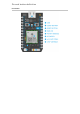

Pin Description
VIN
Thispincanbeusedasaninputoroutput.Asaninput,supply3.6to5.5VDCtopowerthePhoton.When
thePhotonispoweredviatheUSBport,thispinwilloutputavoltageofapproximately4.8VDCduetoa
reversepolarityprotectionseriesSchottkydiodebetweenVUSBandVIN.Whenusedasanoutput,the
maxloadonVINis1A.
RST
Active-lowresetinput.On-boardcircuitrycontainsa1kohmpull-upresistorbetweenRSTand3V3,and
0.1uFcapacitorbetweenRSTandGND.
VBAT SupplytotheinternalRTC,backupregistersandSRAMwhen3V3isnotpresent(1.65to3.6VDC).
3V3
Thispinistheoutputoftheon-boardregulatorandisinternallyconnectedtotheVDDoftheWi-Fi
module.WhenpoweringthePhotonviaVINortheUSBport,thispinwilloutputavoltageof3.3VDC.This
pincanalsobeusedtopowerthePhotondirectly(maxinput3.3VDC).Whenusedasanoutput,themax
loadon3V3is100mA.NOTE:WhenpoweringthePhotonviathispin,ensurepowerisdisconnectedfrom
VINandUSB.
RX
PrimarilyusedasUARTRX,butcanalsobeusedasadigitalGPIOorPWM
[2]
.
TX
PrimarilyusedasUARTTX,butcanalsobeusedasadigitalGPIOorPWM
[2]
.
WKP
Active-highwakeuppin,wakesthemodulefromsleep/standbymodes.WhennotusedasaWAKEUP,
thispincanalsobeusedasadigitalGPIO,ADCinputorPWM
[2]
.Canbereferredtoas A7 whenusedas
anADC.
DAC
12-bitDigital-to-Analog(D/A)output(0-4095),referredtoas DAC or DAC1 insoftware.Canalsobeused
asadigitalGPIOorADC.Canbereferredtoas A6 whenusedasanADC.A3isasecondDACoutput
usedas DAC2 insoftware.
A0~A7
12-bitAnalog-to-Digital(A/D)inputs(0-4095),andalsodigitalGPIOs. A6 and A7 arecodeconvenience
mappings,whichmeanspinsarenotactuallylabeledassuchbutyoumayusecodelike
analogRead(A7) . A6 mapstotheDACpinand A7 mapstotheWKPpin.A4,A5,A7mayalsobeused
asaPWM
[2]
output.
D0~D7
DigitalonlyGPIOpins.D0~D3mayalsobeusedasaPWM
[2]
output.
Notes:
[1]
Inadditiontothe24pinsaroundtheoutsideofthePhoton,thereare7padsonthe
bottomthePhotonPCBthatcanbeusedtoconnecttoextrasignals:RGBLEDoutputs,SETUP
button,SMPSenablelineandUSBD+/D-.PhotonPins#25-31aredescribedinthePinout
diagrams.AlsorefertotheRecommendedPCBlandpatternphotonwithoutheaderssectionfor
theirlocationonthebottomofthePhoton.
[2]
PWMisavailableonD0,D1,D2,D3,A4,A5,WKP,RX,TXwithacaveat:PWMtimerperipheralis
duplicatedontwopins(A5/D2)and(A4/D3)for7totalindependentPWMoutputs.Forexample:
PWMmaybeusedonA5whileD2isusedasaGPIO,orD2asaPWMwhileA5isusedasananalog
input.HoweverA5andD2cannotbeusedasindependentlycontrolledPWMoutputsatthesame
time.
PINDESCRIPTION