
Data Sheet

5
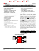
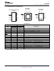
PCA9546A
www.ti.com
SCPS148G –OCTOBER 2005–REVISED MAY 2016
Product Folder Links: PCA9546A
Submit Documentation FeedbackCopyright © 2005–2016, Texas Instruments Incorporated
(1) All typical values are at nominal supply voltage (2.5-V, 3.3-V, or 5-V V
CC
), T
A
= 25°C.
(2) The power-on reset circuit resets the I
2
C bus logic with V
CC
< V
POR
. V
CC
must be lowered to 0.2 V to reset the device.
(3) C
io(ON)
depends on internal capacitance and external capacitance added to the SCn lines when channels(s) are ON.
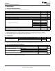
6.4 Electrical Characteristics
over recommended operating free-air temperature range (unless otherwise noted)
PARAMETER TEST CONDITIONS V
CC
MIN TYP
(1)
MAX UNIT
V
POR
Power-on reset voltage
(2)
No load, V
I
= V
CC
or GND V
POR
1.6 2.1 V
V
pass
Switch output voltage V
SWin
= V
CC
, I
SWout
= –100 μA
5 V 3.6
V
4.5 V to 5.5 V 2.6 4.5
3.3 V 1.9
3 V to 3.6 V 1.6 2.8
2.5 V 1.5
2.3 V to 2.7 V 1.1 2
I
OL
SCL, SDA
V
OL
= 0.4 V
2.3 V to 5.5 V
3 7
mA
V
OL
= 0.6 V 6 10
I
I
SCL, SDA
V
I
= V
CC
or GND 2.3 V to 5.5 V
±1
μA
SC3–SC0, SD3–SD0 ±1
A2–A0 ±1
RESET ±1
I
CC
Operating mode f
SCL
= 100 kHz V
I
= V
CC
or GND, I
O
= 0
5.5 V 3 12
μA
3.6 V 3 11
2.7 V 3 10
Standby mode
Low inputs V
I
= GND, I
O
= 0
5.5 V 0.3 1
3.6 V 0.1 1
2.7 V 0.1 1
High inputs V
I
= V
CC
, I
O
= 0
5.5 V 0.3 1
3.6 V 0.1 1
2.7 V 0.1 1
ΔI
CC
Supply-current
change
SCL, SDA
SCL or SDA input at 0.6 V,
Other inputs at V
CC
or GND
8 15
μA
SCL or SDA input at V
CC
– 0.6 V,
Other inputs at V
CC
or GND
2.3 V to 5.5 V 8 15
C
i
A2–A0
V
I
= V
CC
or GND 2.3 V to 5.5 V
4.5 6
pF
RESET 4.5 5.5
C
io(OFF)
(3)
SCL, SDA
V
I
= V
CC
or GND, Switch OFF 2.3 V to 5.5 V
15 19
pF
SC3–SC0, SD3–SD0 6 8
R
ON
Switch on-state resistance
V
O
= 0.4 V, I
O
= 15 mA
4.5 V to 5.5 V 4 9 16
Ω3 V to 3.6 V 5 11 20
V
O
= 0.4 V, I
O
= 10 mA 2.3 V to 2.7 V 7 16 45
6.5 I
2
C Interface Timing Requirements
over recommended operating free-air temperature range (unless otherwise noted) (see Figure 1)
MIN MAX UNIT
I
2
C BUS—STANDARD MODE
f
scl
I
2
C clock frequency 0 100 kHz
t
sch
I
2
C clock high time 4 µs
t
scl
I
2
C clock low time 4.7 µs
t
sp
I
2
C spike time 50 ns
t
sds
I
2
C serial-data setup time 250 ns