
Data Sheet

4
PCA9546A
SCPS148G –OCTOBER 2005–REVISED MAY 2016
www.ti.com
Product Folder Links: PCA9546A
Submit Documentation Feedback Copyright © 2005–2016, Texas Instruments Incorporated
(1) Stresses beyond those listed under Absolute Maximum Ratings may cause permanent damage to the device. These are stress ratings
only, which do not imply functional operation of the device at these or any other conditions beyond those indicated under Recommended
Operating Conditions. Exposure to absolute-maximum-rated conditions for extended periods may affect device reliability.
(2) The input negative-voltage and output voltage ratings may be exceeded if the input and output current ratings are observed.
(3) The package thermal impedance is calculated in accordance with JESD 51-7.
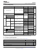
6 Specifications
6.1 Absolute Maximum Ratings
(1)
over operating free-air temperature range (unless otherwise noted)
MIN MAX UNIT
V
CC
Supply voltage –0.5 7 V
V
I
Input voltage
(2)
–0.5 7 V
I
I
Input current ±20 mA
I
O
Output current ±25 mA
Continuous current through V
CC
±100 mA
Continuous current through GND ±100 mA
θ
JA
Package thermal impedance
(3)
D package 73
°C/W
DGV package 120
DW package 57
PW package 108
RGV package 51.38
RGY package 50
P
tot
Total power dissipation 400 mW
T
A
Operating free-air temperature –40 85 °C
T
stg
Storage temperature –65 150
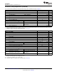
(1) JEDEC document JEP155 states that 500-V HBM allows safe manufacturing with a standard ESD control process.
(2) JEDEC document JEP157 states that 250-V CDM allows safe manufacturing with a standard ESD control process.
6.2 ESD Ratings
VALUE UNIT
V
(ESD)
Electrostatic discharge
Human-body model (HBM), per ANSI/ESDA/JEDEC JS-001
(1)
±2000
V
Charged-device model (CDM), per JEDEC specification JESD22-
C101
(2)
±1000
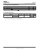
(1) All unused inputs of the device must be held at V
CC
or GND to ensure proper device operation. Refer to the TI application report,
Implications of Slow or Floating CMOS Inputs, SCBA004.
6.3 Recommended Operating Conditions
(1)
MIN MAX UNIT
V
CC
Supply voltage 2.3 5.5 V
V
IH
High-level input voltage
SCL, SDA 0.7 × V
CC
6
V
A2–A0, RESET 0.7 × V
CC
V
CC
+ 0.5
V
IL
Low-level input voltage
SCL, SDA –0.5 0.3 × V
CC
V
A2–A0, RESET –0.5 0.3 × V
CC
T
A
Operating free-air temperature –40 85 °C