
Data Sheet
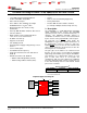
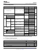
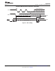

D, DGV, DW, OR PW PACKAGE
(TOP VIEW)
1
2
3
4
5
6
7
8
16
15
14
13
12
11
10
9
A0
A1
RESET
SD0
SC0
SD1
SC1
GND
V
CC
SDA
SCL
A2
SC3
SD3
SC2
SD2
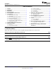
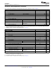
RGY PACKAGE
(TOP VIEW)
2
15
SDAA1
3
14
SCL
RESET
4
13
A2SD0
5
12
SC3SC0
6
11
SD3SD1
7
10
SC2SC1
1
8
A0
GND
16
9
SD2
V
CC
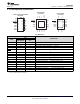
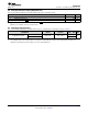
RGV PACKAGE
(TOP VIEW)
8
SC2
13
SDA
16
5
A1
SC1
6
15
A0
GND
V
CC
7
14
SD2
1 12
SCL
RESET
2 11
A2SD0
10
SC3
3
SC0
4
9
SD3SD1
3
PCA9546A
www.ti.com
SCPS148G –OCTOBER 2005–REVISED MAY 2016
Product Folder Links: PCA9546A
Submit Documentation FeedbackCopyright © 2005–2016, Texas Instruments Incorporated
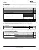
(1) V
DPUX
is the pull-up reference voltage for the associated data line. V
DPUM
is the master I
2
C reference voltage while V
DPU0
- V
DPU3
are
the slave channel reference voltages.
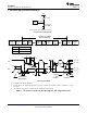
5 Pin Configuration and Functions
Pin Functions
PIN
DESCRIPTION
NAME
NO.
D, DGV, DW,
PW, AND RGY
RGV
A0 1 15 Address input 0. Connect directly to V
CC
or ground
A1 2 16 Address input 1. Connect directly to V
CC
or ground
A2 13 11 Address input 2. Connect directly to V
CC
or ground
GND 8 6 Ground
RESET 3 1
Active low reset input. Connect to V
DPUM
(1)
through a pull-up resistor, if not
used.
SD0 4 2 Serial data 0. Connect to V
DPU0
(1)
through a pull-up resistor
SC0 5 3 Serial clock 0. Connect to V
DPU0
(1)
through a pull-up resistor
SD1 6 4 Serial data 1. Connect to V
DPU1
(1)
through a pull-up resistor
SC1 7 5 Serial clock 1. Connect to V
DPU1
(1)
through a pull-up resistor
SD2 9 7 Serial data 2. Connect to V
DPU2
(1)
through a pull-up resistor
SC2 10 8 Serial clock 2. Connect to V
DPU2
(1)
through a pull-up resistor
SD3 11 9 Serial data 3. Connect to V
DPU3
(1)
through a pull-up resistor.
SC3 12 10 Serial clock 3. Connect to V
DPU3
(1)
through a pull-up resistor
SCL 14 12 Serial clock line. Connect to V
DPUM
(1)
through a pull-up resistor
SDA 15 13 Serial data line. Connect to V
DPUM
(1)
through a pull-up resistor
V
CC
16 14 Supply power