
Data Sheet

19
PCA9546A
www.ti.com
SCPS148G –OCTOBER 2005–REVISED MAY 2016
Product Folder Links: PCA9546A
Submit Documentation FeedbackCopyright © 2005–2016, Texas Instruments Incorporated
10 Power Supply Recommendations
The operating power-supply voltage range of the PCA9546A is 2.3 V to 5.5 V applied at the V
CC
pin. When the
PCA9546A is powered on for the first time or anytime the device must be reset by cycling the power supply, the
power-on reset requirements must be followed to ensure the I
2
C bus logic is initialized properly.
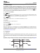
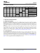
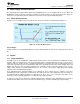
10.1 Power-On Reset Errata
A power-on reset condition can be missed if the V
CC
ramps are outside specification listed in Figure 15.
Figure 15. Power-On Reset Cycle
System Impact
If ramp conditions are outside timing allowances above, POR condition can be missed, causing the device to lock
up.
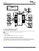
11 Layout
11.1 Layout Guidelines
For PCB layout of the PCA9546A, common PCB layout practices must be followed but additional concerns
related to high-speed data transfer such as matched impedances and differential pairs are not a concern for I
2
C
signal speeds. It is common to have a dedicated ground plane on an inner layer of the board and pins that are
connected to ground must have a low-impedance path to the ground plane in the form of wide polygon pours and
multiple vias. By-pass and de-coupling capacitors are commonly used to control the voltage on the V
CC
pin,
using a larger capacitor to provide additional power in the event of a short power supply glitch and a smaller
capacitor to filter out high-frequency ripple.
In an application where voltage translation is not required, all V
DPUX
voltages and V
CC
could be at the same
potential and a single copper plane could connect all of pull-up resistors to the appropriate reference voltage. In
an application where voltage translation is required, V
DPUM
, V
DPU0
, V
DPU1
, V
DPU2
, and V
DPU3
may all be on the
same layer of the board with split planes to isolate different voltage potentials.
To reduce the total I
2
C bus capacitance added by PCB parasitics, data lines (SCn and SDn) must be a short as
possible and the widths of the traces must also be minimized (e.g. 5-10 mils depending on copper weight).