
Data Sheet

r
p(max)
b
t
R
0.8473 C
=
´
DPUX OL(max)
p(min)
OL
V V
R
I
-
=
17
PCA9546A
www.ti.com
SCPS148G –OCTOBER 2005–REVISED MAY 2016
Product Folder Links: PCA9546A
Submit Documentation FeedbackCopyright © 2005–2016, Texas Instruments Incorporated
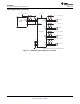
Typical Application (continued)
9.2.1 Design Requirements
The A0, A1, and A2 pins are hardware selectable to control the slave address of the PCA9546A. These pins may
be tied directly to GND or V
CC
in the application.
If multiple slave channels will be activated simultaneously in the application, then the total I
OL
from SCL/SDA to
GND on the master side will be the sum of the currents through all pull-up resistors, R
p
.
The pass-gate transistors of the PCA9546A are constructed such that the V
CC
voltage can be used to limit the
maximum voltage that is passed from one I
2
C bus to another.
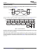
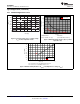
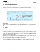
Figure 12 shows the voltage characteristics of the pass-gate transistors (note that the graph was generated using
data specified in the Electrical Characteristics section of this data sheet). In order for the PCA9546A to act as a
voltage translator, the V
pass
voltage must be equal to or lower than the lowest bus voltage. For example, if the
main bus is running at 5 V and the downstream buses are 3.3 V and 2.7 V, V
pass
must be equal to or below 2.7 V
to effectively clamp the downstream bus voltages. As shown in Figure 12, V
pass(max)
is 2.7 V when the PCA9546A
supply voltage is 4 V or lower, so the PCA9546A supply voltage could be set to 3.3 V. Pull-up resistors then can
be used to bring the bus voltages to their appropriate levels (see Figure 11).
9.2.2 Detailed Design Procedure
Once all the slaves are assigned to the appropriate slave channels and bus voltages are identified, the pull-up
resistors, R
p
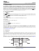
, for each of the buses need to be selected appropriately. The minimum pull-up resistance is a
function of V
DPUX
, V
OL,(max)
, and I
OL
as shown in Equation 1:
(1)
The maximum pull-up resistance is a function of the maximum rise time, t
r
(300 ns for fast-mode operation, f
SCL
=
400 kHz) and bus capacitance, C
b
as shown in Equation 2:
(2)
The maximum bus capacitance for an I
2
C bus must not exceed 400 pF for fast-mode operation. The bus
capacitance can be approximated by adding the capacitance of the PCA9546A, C
io(OFF)
, the capacitance of
wires/connections/traces, and the capacitance of each individual slave on a given channel. If multiple channels
will be activated simultaneously, each of the slaves on all channels will contribute to total bus capacitance.